MAX3748 Ver la hoja de datos (PDF) - Maxim Integrated
Número de pieza
componentes Descripción
Fabricante
MAX3748 Datasheet PDF : 11 Pages
| |||
Compact 155Mbps to 3.2Gbps
Limiting Amplifier
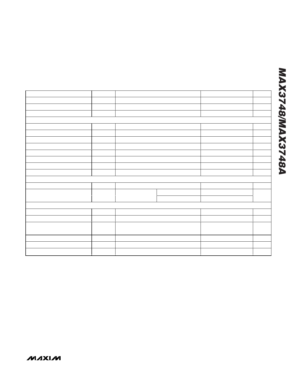
ELECTRICAL CHARACTERISTICS (continued)
(VCC = 2.97V to 3.63V, ambient temperature = -40°C to +85°C, CML output load is 50Ω to VCC, CAZ = 0.1µF, typical values are at
+25°C, VCC = 3.3V, unless otherwise specified. The data input transition time is controlled by a 4th-order Bessel filter with f-3dB =
0.75 ✕ 2.667GHz for all data rates of 2.667Gbps and below, and with f-3dB = 0.75 ✕ 3.2GHz for data rate of 3.2Gbps.)
PARAMETER
SYMBOL
Medium LOS Deassert Level
High LOS Assert Level
High LOS Deassert Level
LOSS OF SIGNAL at 155Mbps (Note 7)
LOS Hysteresis
LOS Assert/Deassert Time
Low LOS Assert Level
Low LOS Deassert Level
Medium LOS Assert Level
Medium LOS Deassert Level
High LOS Assert Level
High LOS Deassert Level
RSSI
RSSI Current Gain (Note 9)
ARSSI
Input-Referred RSSI Current
Stability
TTL/CMOS I/O
LOS Output High Voltage
VOH
LOS Output Low Voltage
VOL
LOS Output Current
RTH = 280Ω
RTH = 80Ω
RTH = 80Ω
CONDITIONS
10log (VDEASSERT/VASSERT)
(Note 8)
RTH = 20kΩ
RTH = 20kΩ
RTH = 280Ω
RTH = 280Ω
RTH = 80Ω
RTH = 80Ω
ARSSI = IRSSI/ICM_RSSI
IRSSI/ARSSI
(Note 10)
ICM_INPUT < 6.6mA
ICM_INPUT > 6.6mA
RLOS = 4.7kΩ to10kΩ to VCC_host (3V)
RLOS = 4.7kΩ to10kΩ to VCC_host (3.6V)
RLOS = 4.7kΩ to10kΩ to VCC_host (3.3V);
IC is powered down
MIN
22.8
TYP
25
38.3
65.2
MAX
38.6
99.3
UNITS
mVP-P
mVP-P
mVP-P
2.1
20
3.5
5.6
13.3
21.2
33.3
55.5
dB
µs
mVP-P
mVP-P
mVP-P
mVP-P
mVP-P
mVP-P
0.03
-31
+33
µA
-73
+90
2.4
V
0.4
V
40
µA
DISABLE Input High
DISABLE Input Low
DISABLE Input Current
VIH
2.0
VIL
RLOS = 4.7kΩ to 10kΩ to VCC_host
V
0.8
V
10
µA
Note 1: Between sensitivity and overload, all AC specifications are met.
Note 2: Guaranteed by design and characterization.
Note 3: The deterministic jitter caused by this filter is not included in the DJ generation specifications (input).
Note 4: 223 - 1 PRBS pattern was substituted by K28.5 pattern to determine the high-speed portion of the deterministic jitter. The
low-speed portion of the DJ (baseline wander) was obtained by measuring the eye width difference between outputs gen-
erated using K28.5 and 223 - 1 PRBS patterns.
Note 5: Random jitter was measured without using a filter at the input.
Note 6: The supply current measurement excludes the CML output currents by connecting the CML outputs to a separate VCC
(see Figure 1).
Note 7: Unless otherwise specified, the pattern for all LOS detect specifications is 223 - 1 PRBS.
Note 8: The signal at the input is switched between two amplitudes, Signal_ON and Signal_OFF, as shown in Figure 2.
Note 9: ICM_INPUT is the input common mode. IRSSI is the current at the RSSI output.
Note 10: Stability is defined as variation over temperature and power supply with respect to the typical gain of the part.
_______________________________________________________________________________________ 3
Share Link: 