ML6509CS Ver la hoja de datos (PDF) - Micro Linear Corporation
Número de pieza
componentes Descripción
Fabricante
ML6509CS Datasheet PDF : 10 Pages
| |||
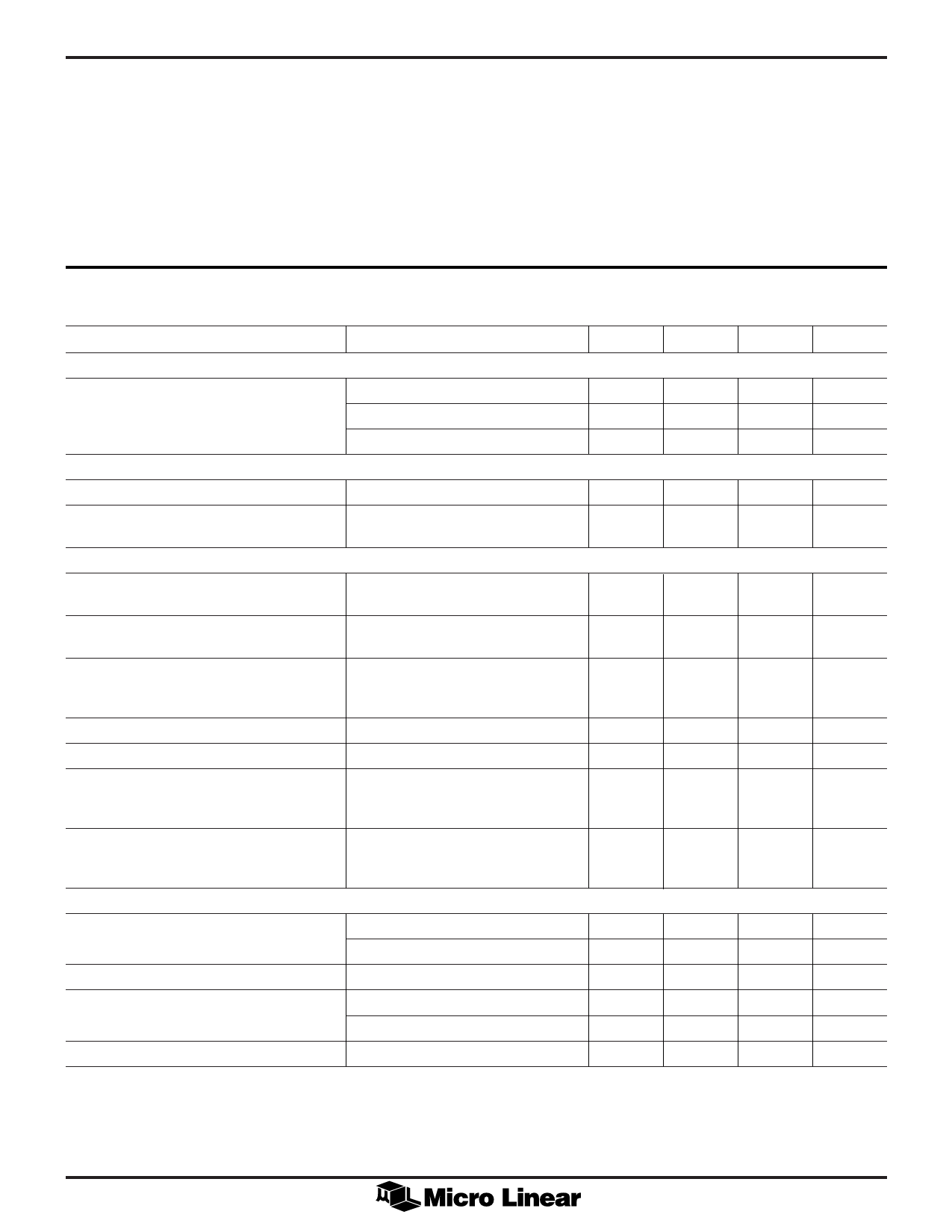
ABSOLUTE MAXIMUM RATINGS
Signal Line Voltage ............................. –0.3 to TERMPWR +0.3V
Regulator Output Current ................................... –100 to 300mA
TERMPWR Voltage ..................................................... –0.3 to 7V
Storage Temperature .......................................... –65°C to 150°C
Soldering Temperature ..................................... 260°C for 10 sec
Thermal Impedance (qJA)
SOIC .......................................................................... 95°C/W
TSSOP ...................................................................... 110°C/W
ML6509
OPERATING CONDITIONS
TERMPWR Voltage .................................................. 4V to 5.25V
Operating Temperature ........................................... 0°C to 70°C
ELECTRICAL CHARACTERISTICS
Unless otherwise stated, these specifications apply for 4V - TERMPWR - 5.25V, and TA = 0°C to 70°C (Note 1)
PARAMETER
CONDITIONS
MIN
TYP
MAX
SUPPLY
TERMPWR Supply Current
L1–L9 = open, DISCNKT = open
3.5
5
L1–L9 = 0.2 V, DISCNKT = open
225
250
DISCNKT = 0 (active)
70
100
DISCNKT
Input Low Voltage
LPWR, DISCNKT
1.0
Input High Voltage
LPWR, DISCNKT
TERMPWR
–1.0
OUTPUT
Output High Voltage
Measuring each signal line while
other eight are high
2.8
2.85
2.9
Maximum Output Current
VOUT = 0.2V, Measuring each signal
20
24
(Normal Mode)
line while the other eight are high
Maximum Output Current
(Lowpower Mode)
VOUT = 0.2V, LPWR = 0, and
0.8
1
1.2
measuring each signal line while the
other eight are high
Output Clamp Level
IOUT = –30mA
–0.15
0
0.15
Current Sink Capability
Output Capacitance
(ML Method)
VOUT = 3.2V (per line)
7
12
L1 thru L9, DISCNKT = 0
2VP-P 100kHz square wave applied
biased at 1V D.C.
4
5
Output Capacitance
(X3T9.2/855D method)
L1 thru L9, DISCNKT = 0
0.4VP-P, 1MHz square wave applied
biased at 0.5V D.C.
6
7
REGULATOR
Output Voltage
Sourcing 0–200mA
2.8
2.85
2.9
Sinking 0–50mA
2.8
2.85
2.95
Dropout Voltage
L1–L9 = 0.2V, VOUT = 2.85V
1.0
1.2
Short Circuit Current
Regulator output = 0V
100
Regulator output = 5V
300
Thermal Shutdown
170
Note 1: Limits are guaranteed by 100% testing, sampling, or correlation with worst case test conditions.
UNITS
mA
mA
µA
V
V
V
mA
mA
V
mA
pF
pF
V
V
V
mA
mA
°C
3
Share Link: 