HV518 Ver la hoja de datos (PDF) - Supertex Inc
Número de pieza
componentes Descripción
Fabricante
HV518 Datasheet PDF : 5 Pages
| |||
HV518
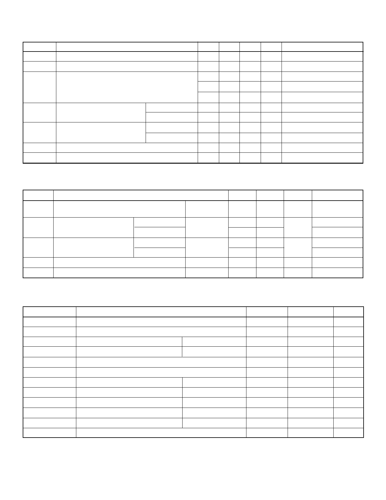
Electrical Characteristics
(over recommended ranges of operating free-air temperature and VDD. Unless otherwise noted, VPP = 80V)
Symbol
Parameter
Min Typ Max Units
Conditions
IDD
Supply current
IDDQ
Quiescent supply current
IPP
Supply current
10
0.5
12
7 10
500
mA VDD = 5V, fCH = 6.0 MHz
mA VDD = 5.5V, VIN = 0V
mA Output high, TA = -40°C
mA Output high, TA = 0 to +85°C
µA Outputs low
VOH
High-level output voltage
HVoutput
Serial output
70.0
4.5 4.9
5
VOL
Low-level output
HVoutput
Serial output
5
0.06 0.8
IIH
High-level logic input current
0.1
1
IIL
Low-level logic input current
-0.1 -1
Note: The total number of ON outputs times the duty cycle must not exceed the allowable package power disspation.
V
IOH= -25mA
V
VDD = 5V, IOH = -20µA
V
IOL= 1mA
V
IOL =20µA
µA VIH = VDD
µA VIL = 0V
Switching Characteristics (VPP = 80V, CL = 50 pF, TA = 25°C, unless otherwise noted)
Symbol Parameter
Min
Max
Unit
Conditions
td
Delay time, Clock to data output
VDD = 4.5V
600
ns
CL =15 pF
See Figure 4
tDHL
Delay time, high-to-low-level, from latch enable VDD = 4.5V
HVoutput
from strobe
1.5
µs
See Figure 5
1
See Figure 6
tDLH
Delay time, low-to-high-level from latch enable VDD = 4.5V
HVoutput
from strobe
1.5
µs
See Figure 5
1
See Figure 6
tTHL
Transition time, high-to-low-level, HVoutput
tTLH
Transition time, low-to-high-level, HVoutput
VDD = 4.5V
VDD = 4.5V
3
µs
See Figure 6
2.5
µs
See Figure 6
Recommended Operating Conditions (TA = 25°C, unless otherwise noted)
Symbol
Parameter
Min
Max
VDD
Logic voltage supply
4.5
5.5
VPP
High voltage supply
8
80
VIH
High-level input voltage (See Fig.3.)
VDD = 4.5V
3.5
VIL
Low-level input voltage (See Fig. 3.)
VDD = 4.5V
1
IOH
High-level output current
-25
IOL
Low-level output current
2
fCLK
Clock frequency (see Figure 3)
VDD = 4.5V
6.0
tw(CKH)
Pulse duration , clock high
VDD = 4.5V
83
tw(CKL)
Pulse duration , clock low
VDD = 4.5V
83
tsu
Setup time, data before clock
VDD = 4.5V
75
th
Hold time, data after clock
VDD = 4.5V
75
TA
Operating free-air temperature
-40
85
Note:
Power-up sequence should be the following:
1. Connect ground.
2. Apply VDD.
3. Set all inputs (Data, CLK, Enable, etc.) to a known state.
4. Apply VPP.
5. The VPP should not drop below VDD or float during operation.
Power-down sequence should be the reverse of the above.
2
Units
V
V
V
V
mA
mA
MHz
ns
ns
ns
ns
°C
Share Link: 