HV57009 Ver la hoja de datos (PDF) - Supertex Inc
Número de pieza
componentes Descripción
Fabricante
HV57009 Datasheet PDF : 7 Pages
| |||
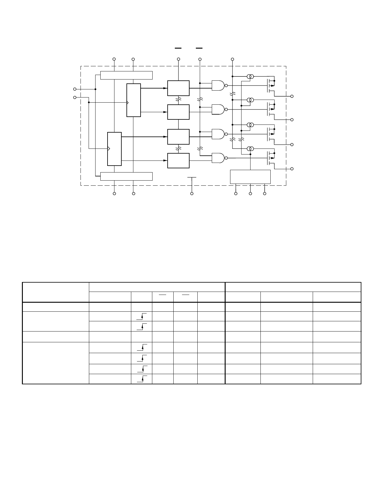
Figure 3: Functional Block Diagram
DIR
CLK
DI/O2A DI/O1A
I/O
SR1
LE BL
VDD
Latch
Latch
SR2
I/O
Latch
Latch
Programmable
Current
DI/O2B DI/O1B
VSS
VBP +IN -IN
Note: Each SR (shift register) provides 32 outputs. SR1 supplies outputs 1 to 32 and SR2 supplies outputs 33 to 64.
HV57009
HVOUT1
HVOUT2
HVOUT3
•
•
•
HVOUT32
HVOUT33
HVOUT34
HVOUT35
•
•
•
HVOUT64
Figure 4: Function Table
Inputs
Function
All O/P High
Data In
X
CLK LE
BL
X
X
L
DIR Shift Reg
X
*
Data Falls Through
L
(Latches Tansparent)
H
H
H
H
H
X
L....L
X
H....H
Data Stored in Latches
X
X
L
H
X
*
I/O Relation
D 1-2A
I/O
DI/O1-2A
D 1-2B
I/O
DI/O1-2B
H
H
L
H
L
H
H
H
H
Qn→Qn+1
H
Qn→Qn+1
L
Qn→Qn-1
L
Qn→Qn-1
Notes:
* = dependent on previous stage’s state. See Figure 7 for DIN and DOUT pin designation for CW and CCW shift.
H = VDD (Logic)/VNN (HV Outputs)
L = VSS
Outputs
HV Outputs
ON
ON
OFF
Inversion of
Stored Data
New ON or OFF
Previous ON or OFF
Previous ON or OFF
New ON or OFF
Data Out
*
L
H
*
D 1-2B
I/O
DI/O1-2B
D 1-2A
I/O
DI/O1-2A
5
Share Link: 