LT1280A Ver la hoja de datos (PDF) - Linear Technology
NĂșmero de pieza
componentes DescripciĂłn
Fabricante
LT1280A Datasheet PDF : 8 Pages
| |||
LT1280A/LT1281A
ELECTRICAL CHARACTERISTICS (Note 2)
PARAMETER
CONDITIONS
MIN TYP MAX
UNITS
Logic Input Current
Output Short-Circuit Current
Output Leakage Current
Data Rate (Note 7)
Slew Rate
Propagation Delay
Receiver
0.8V †VIN †2.0V
VOUT = 0V
Shutdown VOUT = ±30V (Note 4)
RL = 3k, CL = 2500pF
RL = 3k, CL = 1000pF
RL = 3k, CL = 51pF
RL = 3k, CL = 2500pF
Output Transition tHL High-to-Low (Note 5)
Output Transition tLH Low-to-High
q
5
20
±9
17
q
10
100
120
250
15
30
4
7
0.6
1.3
0.5
1.3
”A
mA
”A
kBaud
kBaud
V/”s
V/”s
”s
”s
Input Voltage Thresholds
Input Low Threshold (VOUT = High)
Input High Threshold (VOUT = Low)
Input Low
Input High
C Grade
q 0.8
1.3
V
C Grade
q
1.7
2.4
V
I Grade
q 0.2
1.3
V
I Grade
q
1.7
3.0
V
Hysteresis
q 0.1
0.4
1.0
V
Input Resistance
Output Leakage Current
Output Voltage
Output Short-Circuit Current
Propagation Delay
VIN = ±10V
Shutdown (Note 4) 0 †VOUT †VCC
Output Low, IOUT = â 1.6mA
Output High, IOUT = 160”A (VCC = 5V)
Sinking Current, VOUT = VCC
Sourcing Current, VOUT = 0V
Output Transition tHL High-to-Low (Note 6)
Output Transition tLH Low-to-High
3
5
7
kâŠ
q
1
10
”A
q
0.2
0.4
V
q 3.5
4.2
V
â 20 â 10
mA
10
20
mA
250 600
ns
350 600
ns
The q denotes specifications which apply over the operating temperature
range (0°C †TA †70°C for commercial grade, and â 40°C †TA †85°C for
industrial grade.
Note 1: Absolute Maximum Ratings are those values beyond which the life
of the device may be impaired.
Note 2: Testing done at VCC = 5V and VON/OFF = 3V, unless otherwise
specified.
Note 3: Supply current is measured as the average over several charge
pump cycles. C + = C â = C1 = C2 = 0.1”F. All outputs are open, with all
driver inputs tied high.
Note 4: Supply current measurements in shutdown are performed with
VON/OFF †0.1V.
Note 5: For driver delay measurements, RL = 3k and CL = 51pF. Trigger
points are set between the driverâs input logic threshold and the output
transition to the zero crossing (tHL = 1.4V to 0V and tLH = 1.4V to 0V).
Note 6: For receiver delay measurements, CL = 51pF. Trigger points are
set between the receiverâs input logic threshold and the output transition
to standard TTL/CMOS logic threshold (tHL = 1.3V to 2.4V and tLH = 1.7V
to 0.8V).
Note 7: Data rate operation guaranteed by slew rate, short-circuit current
and propagation delay tests.
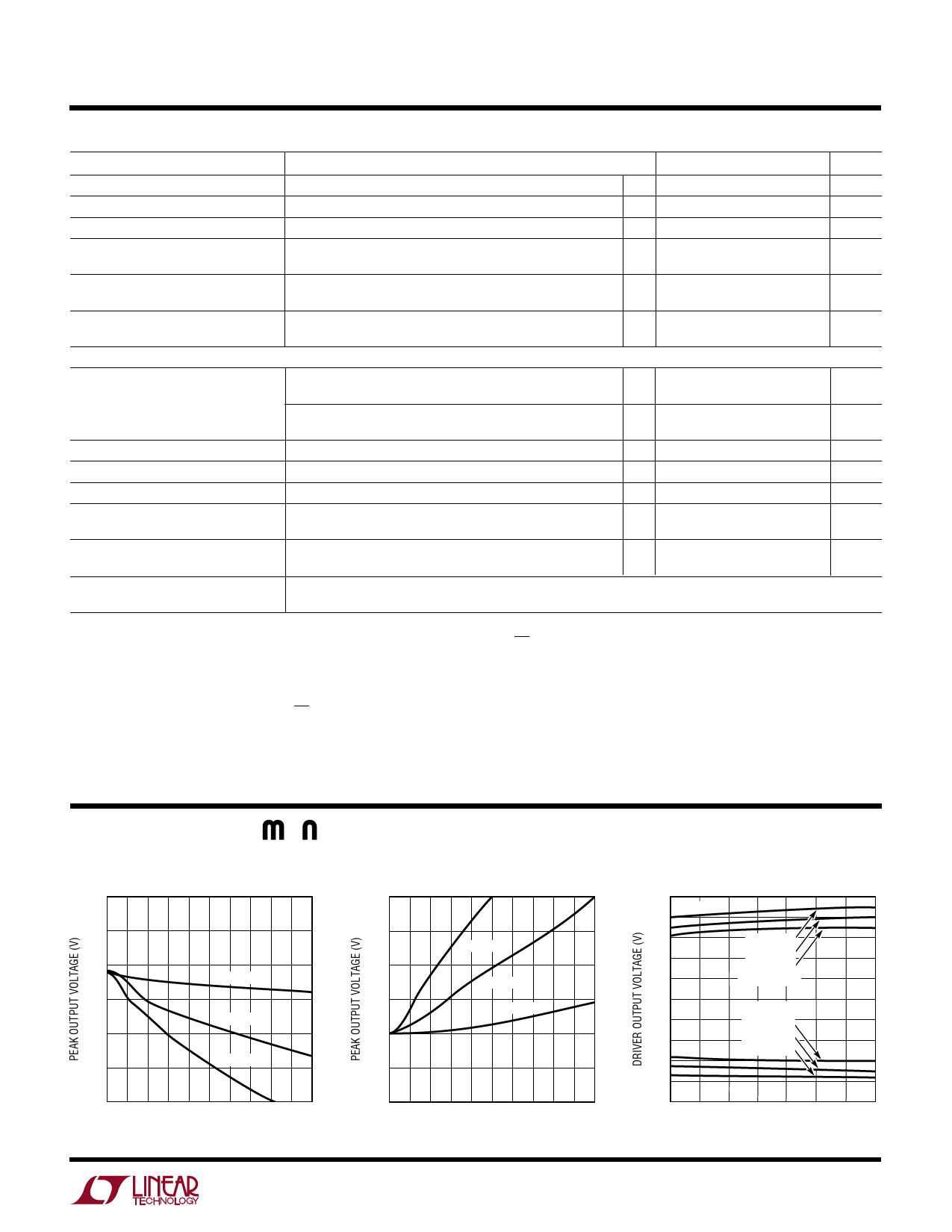
TYPICAL PERFOR A CE CHARACTERISTICS
Driver Maximum Output Voltage
vs Load Capacitance
8.0
Driver Minimum Output Voltage
vs Load Capacitance
â4.0
7.5
â4.5
120k BAUD
7.0
â5.0
20k BAUD
60k BAUD
6.5
â5.5
20k BAUD
60k BAUD
6.0
â6.0
120k BAUD
5.5
â6.5
5.0
01
2 345678
LOAD CAPACITANCE (nF)
9 10
LT1280A âą TPC01
â7.0
01
2 345678
LOAD CAPACITANCE (nF)
9 10
LT1280A âą TPC02
Driver Output Voltage
10
8 RL = 3k
6
VCC = 5.5V
4
VCC = 5V
VCC = 4.5V
2
OUTPUT HIGH
0
OUTPUT LOW
â2
VCC = 4.5V
â4
VCC = 5V
VCC = 5.5V
â6
â8
â10
â55 â25
0 25 50 75
TEMPERATURE (°C)
100 125
LT1280A âą TPC03
3
Share Link: 