MB40C328PFV Ver la hoja de datos (PDF) - Fujitsu
Número de pieza
componentes Descripción
Fabricante
MB40C328PFV Datasheet PDF : 16 Pages
| |||
MB40C328
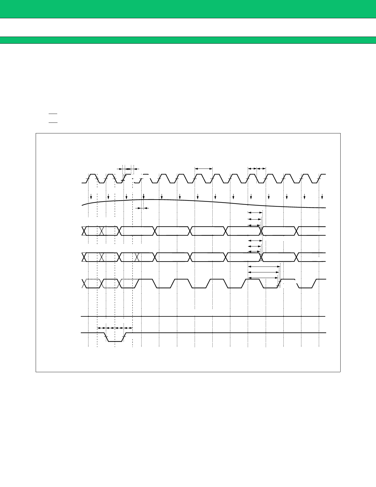
s TIMING CHART 2
CLK input-demultiplex output (in-phase) mode
• CLK = 100 MHz (max)
• CLKA = CLKB = “L” (DVSS)
• CKSEL = “H” (AVDD)
• DSEL = “L” (DVSS)
• CE = “L” (AVSS)
• OE = “L” (DVSS)
VIHD
CLK input
VILD
tr
tf
T
tWS+ tWS−
DVDD − 0.5 V
0.5 V
1.5 V
N−1 N−2 N−1 N
N + 1 N + 2 N + 3 N + 4 N + 5 N + 6 N + 7 N + 8 N + 9 N + 10
VINA input
tAD
N−9 N−9
VOHD or N − 10 or N − 8
DA0 to DA7
VOLD
N−7
or N − 8
N − 10 N − 10 N − 8 N − 8
VOHD or N − 11 or N − 9or N − 9 or N − 7
DB0 to DB7
VOLD
N−5
or N − 6
N−6
or N − 7
VOHD
CLKOA
VOLD
N−3
or N − 4
N−4
or N − 5
tpdM1(max)
tpdM1(typ)
tpdM1(min)
N+1
N−1
or N − 2
DVDD − 0.4 V
0.4V
tpdM1(max)
tpdM1(typ)
tpdM1(min)
N
N−2
DVDD − 0.4 V
or N − 3 0.4V
tpdM1O(max)
tpdM1O(typ)
tpdM1O(min)
N+3
N+2
DVDD − 0.4 V
0.4 V
VOHD
CLKOB
VOLD
VIHD
RESET input
VILD
th tS th tS
1.5 V
ALL “L” fix
• VINA input — Sampling at CLK rising
• DA0 to DA7 — Output (after 5 CLK + tpdM1 from Sampling) at CLK rising
• DB0 to DB7 — Output (after 6 CLK + tpdM1 from Sampling) at CLK rising
10
Share Link: 