EL4585CN Ver la hoja de datos (PDF) - Elantec -> Intersil
Número de pieza
componentes Descripción
Fabricante
EL4585CN Datasheet PDF : 16 Pages
| |||
EL4585C
Horizontal Genlock 8 FSC
creases Ti decreases For LDET to be low at
l l lock Ti k 50nS C4 is used mainly to attenuate
high frequency noise from the charge pump The
effect these components have on time to lock is
illustrated below
Lock Time
Let TeR3C3 As T increases damping increases
but so does lock time Decreasing T decreases
damping and speeds up loop response but in-
creases overshoot and thus increases the number
of hunting oscillations before lock Critical damp-
ing (ge1) occurs at minimum lock time Because
decreased damping also decreases loop stability
it is sometimes desirable to design slightly over-
damped (gl1) trading lock time for increased
stability
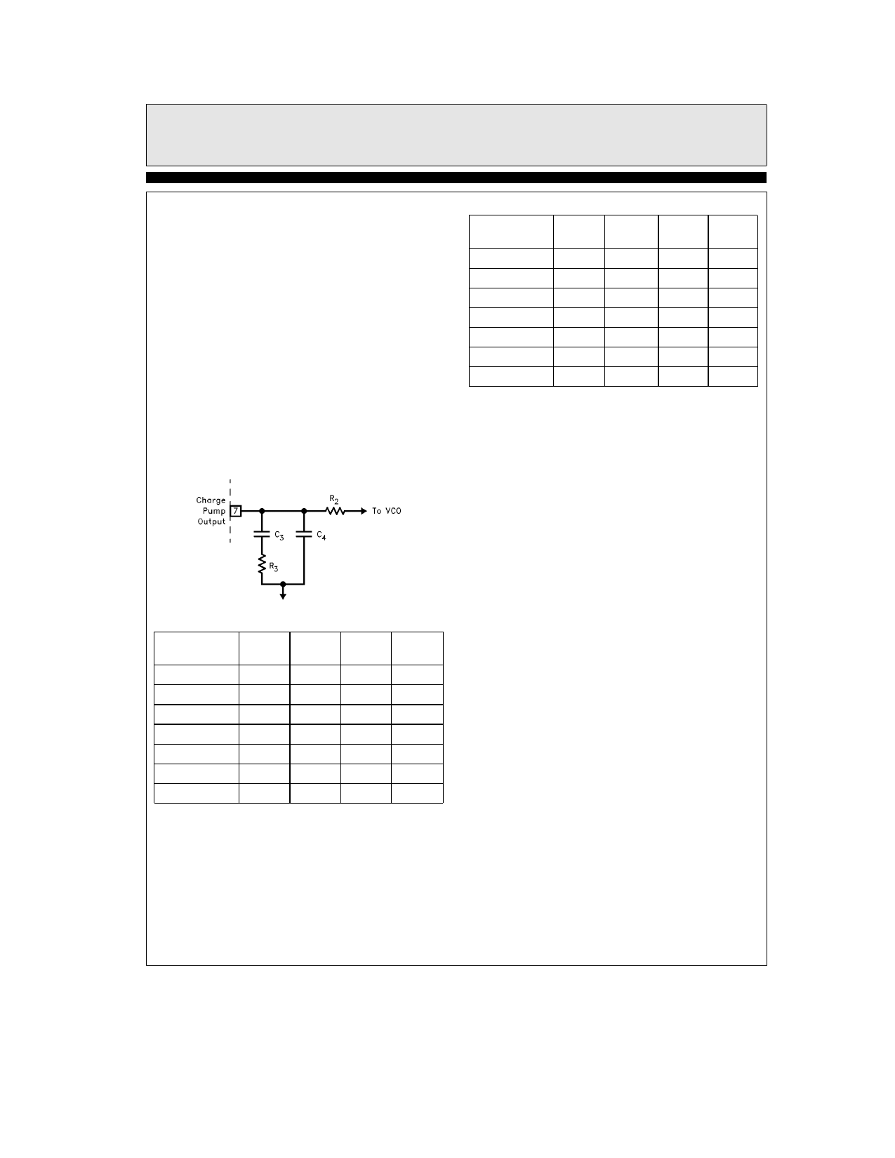
Typical Loop Filter
4585 – 16
LC Loop Filter Components (Approximate)
Frequency
(MHz)
R2
(kX)
R3
(kX)
C3
(mF)
C4
(mF)
26 602
100
39
0 01
0 001
27 0
100
39
0 01
0 001
29 5
100
43
0 01
0 001
35 468
100
51
0 01
0 001
21 476
100
30
0 01
0 001
24 546
100
36
0 01
0 001
28 636
100
43
0 01
0 001
Xtal Loop Filter Components (Approximate)
Frequency
(MHz)
R2
(kX)
R3
(MX)
C3
(pF)
C4
(pF)
26 602
100
43
68
68
27 0
100
43
68
68
29 5
100
43
68
68
35 468
100
43
68
68
21 476
100
43
68
68
24 546
100
43
68
68
28 636
100
43
68
68
PCB Layout Considerations
It is highly recommended that power and ground
planes be used in layout The oscillator and filter
sections constitute a feedback loop and thus care
must be taken to avoid any feedback signal influ-
encing the oscillator except at the control input
The entire oscillator filter section should be sur-
rounded by copper ground to prevent unwanted
influences from nearby signals Use separate
paths for analog and digital supplies keeping the
analog (oscillator section) as short and free from
spurious signals as possible Careful attention
must be paid to correct bypassing Keep lead
lengths short and place bypass caps as close to
the supply pins as possible If laying out a PCB
to use discrete components for the VCO section
care must be taken to avoid parasitic capacitance
at the OSC pins 3 and 5 and FILTER out (pin
7) Remove ground and power plane copper
above and below these traces to avoid making a
capacitive connection to them It is also recom-
mended to enclose the oscillator section within a
shielded cage to reduce external influences on the
VCO as they tend to be very sensitive to ‘‘hand
waving’’ influences the LC variety being more
sensitive than crystal controlled oscillators In
general the higher the operating frequency the
more important these considerations are Self
contained VCXO or VCO modules are already
mounted in a shielding cage and therefore do not
require as much consideration in layout Many
crystal manufacturers publish informative litera-
ture regarding use and layout of oscillators which
should be helpful
11
Share Link: 