BU208A Ver la hoja de datos (PDF) - ON Semiconductor
Número de pieza
componentes Descripción
Fabricante
BU208A Datasheet PDF : 8 Pages
| |||
BU208A
BASE DRIVE
The Key to Performance
By now, the concept of controlling the shape of the turn–off base
current is widely accepted and applied in horizontal deflection
design. The problem stems from the fact that good saturation of the
output device, prior to turn–off, must be assured. This is
accomplished by providing more than enough IB1 to satisfy the
lowest gain output device hFE at the end of scan ICM. Worst–case
component variations and maximum high voltage loading must
also be taken into account.
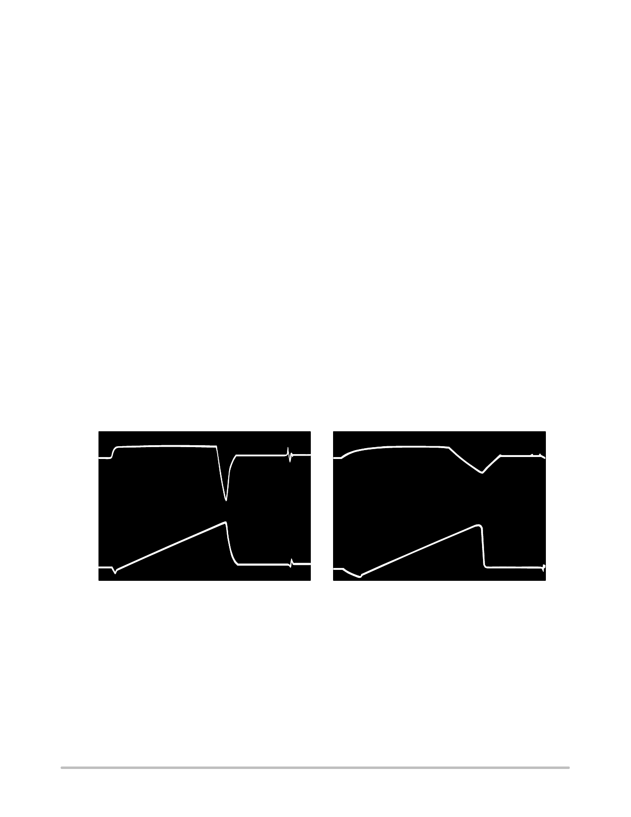
If the base of the output transistor is driven by a very low
impedance source, the turn–off base current will reverse very
quickly as shown in Figure 3. This results in rapid, but only partial
collector turn–off, because excess carriers become trapped in the
high resistivity collector and the transistor is still conductive. This
is a high dissipation mode, since the collector voltage is rising very
rapidly. The problem is overcome by adding inductance to the base
circuit to slow the base current reversal as shown in Figure 4, thus
allowing access carrier recombination in the collector to occur
while the base current is still flowing.
Choosing the right LB Is usually done empirically since the
equivalent circuit is complex, and since there are several important
variables (ICM, IB1, and hFE at ICM). One method is to plot fall time
as a function of LB, at the desired conditions, for several devices
within the hFE specification. A more informative method is to plot
power dissipation versus IB1 for a range of values of LB.
This shows the parameter that really matters, dissipation,
whether caused by switching or by saturation. For very low LB a
very narrow optimum is obtained. This occurs when IB1 hFE ^
ICM, and therefore would be acceptable only for the “typical”
device with constant ICM. As LB is increased, the curves become
broader and flatter above the IB1. hFE = ICM point as the turn off
“tails” are brought under control. Eventually, if LB is raised too far,
the dissipation all across the curve will rise, due to poor initiation
of switching rather than tailing. Plotting this type of curve family
for devices of different hFE, essentially moves the curves to the
left, or right according to the relation IB1 hFE = constant. It then
becomes obvious that, for a specified ICM, an LB can be chosen
which will give low dissipation over a range of hFE and/or IB1. The
only remaining decision is to pick IB1 high enough to
accommodate the lowest hFE part specified. Neither LB nor IB1 are
absolutely critical. Due to the high gain of ON Semiconductor
devices it is suggested that in general a low value of IB1 be used to
obtain optimum efficiency — eg. for BU208A with ICM = 4.5 A
use IB1 [ 1.5 A, at ICM = 4 A use IB1 [ 1.2 A. These values are
lower than for most competition devices but practical tests have
showed comparable efficiency for ON Semiconductor devices
even at the higher level of IB1.
An LB of 10 µH to 12 µH should give satisfactory operation of
BU208A with ICM of 4 to 4.5 A and IB1 between 1.2 and 2 A.
TEST CIRCUIT WAVEFORMS
IB
IB
IC
(TIME)
Figure 3.
IC
(TIME)
Figure 4.
TEST CIRCUIT OPTIMIZATION
The test circuit may be used to evaluate devices in the
conventional manner, i.e., to measure fall time, storage time, and
saturation voltage. However, this circuit was designed to evaluate
devices by a simple criterion, power supply input. Excessive
power input can be caused by a variety of problems, but it is the
dissipation in the transistor that is of fundamental importance.
Once the required transistor operating current is determined, fixed
circuit values may be selected.
http://onsemi.com
4
Share Link: 