LC75878W(2013) Ver la hoja de datos (PDF) - ON Semiconductor
Número de pieza
componentes Descripción
Fabricante
LC75878W Datasheet PDF : 35 Pages
| |||
LC75878W
Electrical Characteristics for the Allowable Operating Ranges
Parameter
Symbol
Conditions
Ratings
unit
min
typ
max
Hysteresis
Input high level current
VH
CE, CL, DI, INH
IIH
CE, CL, DI, INH: VI=6.0V
0.1VDD
V
5.0
μA
Input low level current
IIL
CE, CL, DI, INH: VI=0V
-5.0
μA
Output high level voltage
VOH1
S1 to S75: IO=-20μA
VLCD0-0.6
VOH2
COM1 to COM10: IO=-100μA
VLCD0-0.6
V
VOH3
P1 to P4: IO=-1mA
VDD-1.0
Output low level voltage
VOL1
S1 to S75: IO=20μA
VLCD4+0.6
VOL2
COM1 to COM10: IO=100μA
VLCD4+0.6
V
VOL3
P1 to P4: IO=1mA
1.0
Output middle level voltage
*1
VMID1
S1 to S75: IO=±20μA
2/4(VLCD0
-VLCD4)
-0.6
2/4(VLCD0
-VLCD4)
+0.6
VMID2
COM1 to COM10: IO=±100μA
3/4(VLCD0
-VLCD4)
-0.6
3/4(VLCD0
-VLCD4)
V
+0.6
VMID3
COM1 to COM10: IO=±100μA
1/4(VLCD0
-VLCD4)
-0.6
1/4(VLCD0
-VLCD4)
+0.6
Oscillator frequency
fOSC
OSC: ROSC=43kΩ, COSC=680pF
40
50
60 kHz
Current drain
IDD1
VDD: Power saving mode
5
IDD2
ILCD1
VDD: VDD=6.0V, Outputs open
fOSC=50kHz
VLCD: Power saving mode
200
400
5
ILCD2
VLCD: VLCD=11.0V
Outputs open
fOSC=50kHz
When the display contrast adjustment circuit is
500
1000
μA
used.
ILCD3
VLCD: VLCD=11.0V
Outputs open
fOSC=50kHz
When the display contrast adjustment circuit is
250
500
not used.
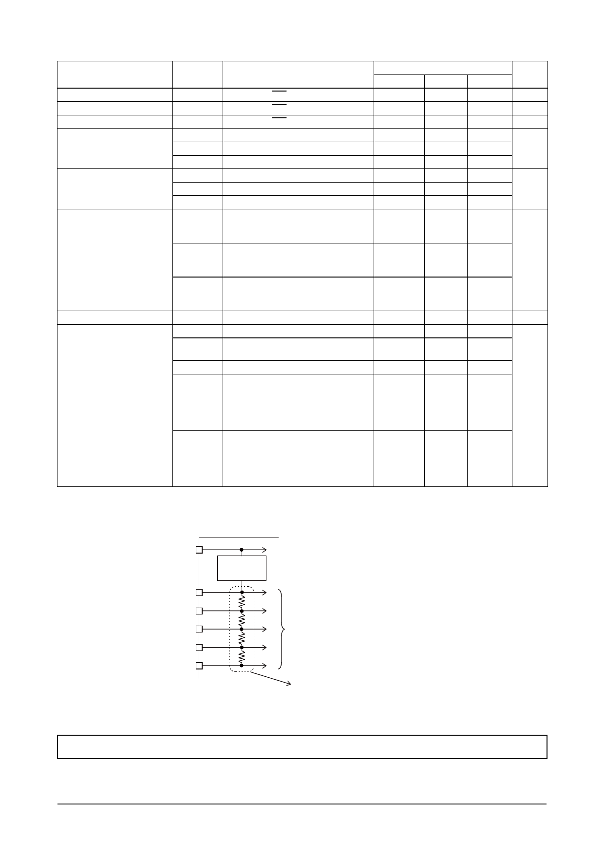
Note: *1. Excluding the bias voltage generation divider resistor built into VLCD0, VLCD1, VLCD2, VLCD3, and
VLCD4. (See Figure 1.)
VLCD
VLCD0
VLCD1
VLCD2
VLCD3
VLCD4
CONTRAST
ADJUSTER
To the common and segment drivers
Excluding these resistors
Figure 1
No.6473-3/35
Share Link: 