FL7930BMX_G Ver la hoja de datos (PDF) - Fairchild Semiconductor
Número de pieza
componentes Descripción
Fabricante
FL7930BMX_G
Fairchild Semiconductor

FL7930BMX_G Datasheet PDF : 24 Pages
| |||
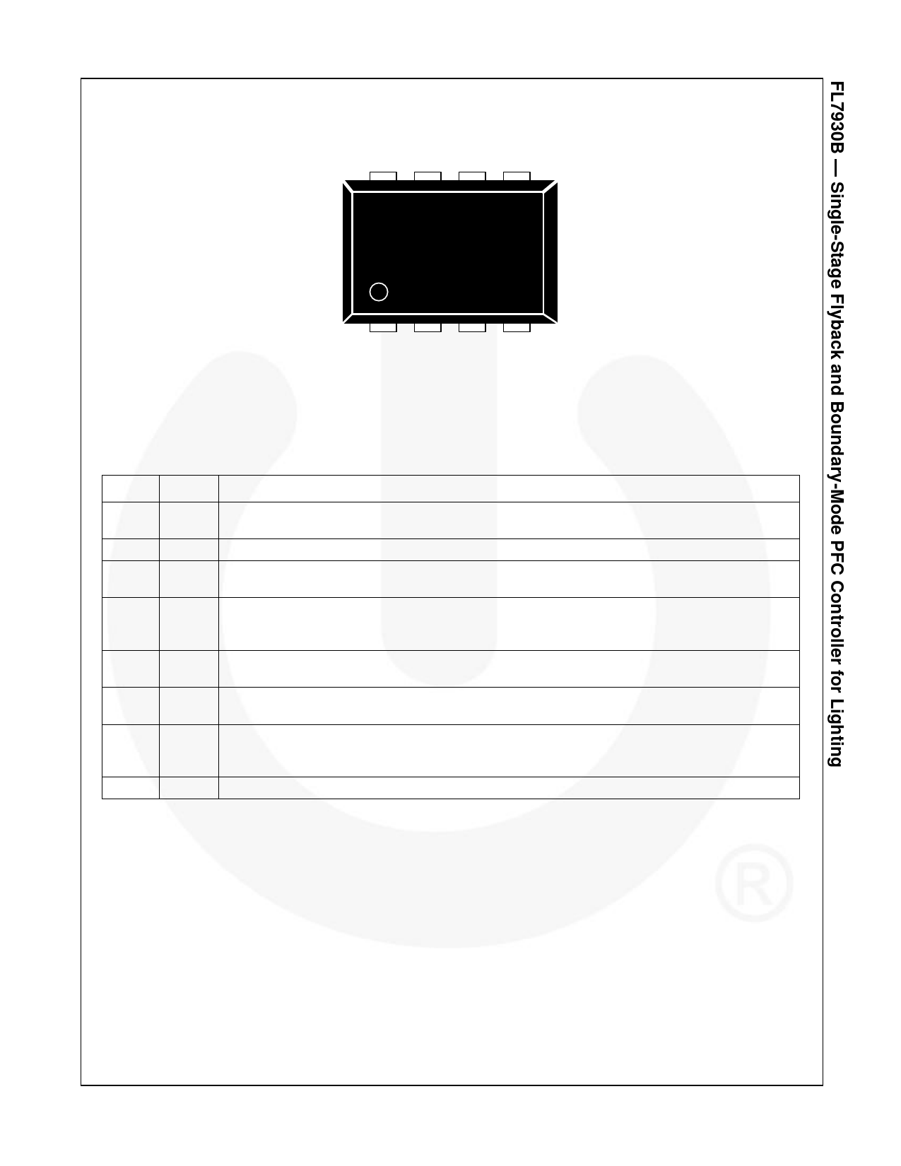
Pin Configuration
VCC OUT GND ZCD
FL7930BG
8-SOP
INV OVP COMP CS
Figure 4. Pin Configuration (Top View)
Pin Definitions
Pin #
1
2
3
4
5
6
7
8
Name
Description
INV
This pin is the inverting input of the error amplifier. The output voltage of the boost PFC converter
should be resistively divided to 2.5 V.
OVP This pin is used to detect PFC output over voltage when INV pin information is not correct.
COMP
This pin is the output of the transconductance error amplifier. Components for the output voltage
compensation should be connected between this pin and GND.
This pin is the input of the over-current protection comparator. The MOSFET current is sensed
CS using a sensing resistor and the resulting voltage is applied to this pin. An internal RC filter is
included to filter switching noise.
ZCD
This pin is the input of the zero-current detection (ZCD) block. If the voltage of this pin goes
higher than 1.5 V, then goes lower than 1.4 V, the MOSFET is turned on.
GND
This pin is used for the ground potential of all the pins. For proper operation, the signal ground
and the power ground should be separated.
OUT
This pin is the gate drive output. The peak sourcing and sinking current levels are +500 mA and
-800 mA, respectively. For proper operation, the stray inductance in the gate driving path must be
minimized.
VCC This is the IC supply pin. IC current and MOSFET drive current are supplied using this pin.
© 2010 Fairchild Semiconductor Corporation
FL7930B • Rev. 1.0.4
4
www.fairchildsemi.com
Share Link: