HM-6642/883 Ver la hoja de datos (PDF) - Intersil
Número de pieza
componentes Descripción
Fabricante
HM-6642/883 Datasheet PDF : 9 Pages
| |||
HM-6642/883
Absolute Maximum Ratings
Supply Voltage . . . . . . . . . . . . . . . . . . . . . . . . . . . . . . . . . . . . . +7.0V
Input, Output or I/O Voltage . . . . . . . . . . . . GND-0.3V to VCC+0.3V
Typical Derating Factor . . . . . . . . . . . 5mA/MHz Increase in ICCOP
ESD Classification . . . . . . . . . . . . . . . . . . . . . . . . . . . . . . . . . Class 1
Operating Conditions
Operating Voltage Range . . . . . . . . . . . . . . . . . . . . . . . . +4.5V to +5.5V
Operating Temperature Range . . . . . . . . . . . . . . . .-55°C to +125°C
Input Low Voltage . . . . . . . . . . . . . . . . . . . . . . . . . . . -0.3V to +0.8V
Input High Voltage . . . . . . . . . . . . . . . . . . . . . . . . . 2.4 to VCC+0.3V
Thermal Information
Thermal Resistance (Typical)
θJA (°C/W) θJC (°C/W)
SBDIP Package . . . . . . . . . . . . . . . . . .
52
14
Slim SBDIP . . . . . . . . . . . . . . . . . . . . .
70
19
CLCC Package . . . . . . . . . . . . . . . . . .
58
14
Maximum Storage Temperature Range . . . . . . . . . .-65°C to +150°C
Maximum Junction Temperature . . . . . . . . . . . . . . . . . . . . . . +175°C
Maximum Lead Temperature (Soldering 10s) . . . . . . . . . . . . +300°C
Die Characteristics
Gate Count . . . . . . . . . . . . . . . . . . . . . . . . . . . . . . . . . . .1680 Gates
CAUTION: Stresses above those listed in “Absolute Maximum Ratings” may cause permanent damage to the device. This is a stress only rating and operation of the
device at these or any other conditions above those indicated in the operational sections of this specification is not implied.
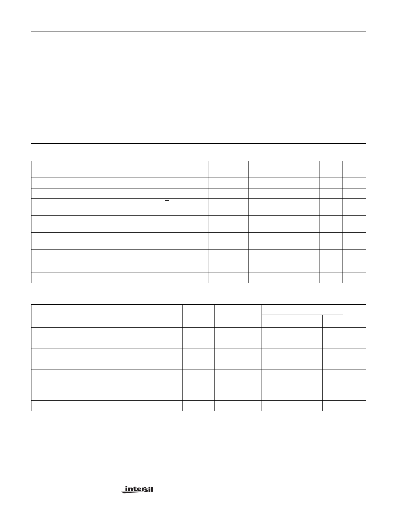
TABLE 1. HM-6642/883 DC ELECTRICAL PERFORMANCE SPECIFICATIONS
Device Guaranteed and 100% Tested
PARAMETER
SYMBOL
(NOTES 1, 4)
CONDITIONS
GROUP A TEMPERATURE
SUBGROUPS
(°C)
MIN
High Level Output Voltage
Low Level Output Voltage
High Impedance Output
Leakage Current
VOH
VOL
IIOZ
VCC = 4.5V, IO = -1.0mA
VCC = 4.5V, IO = +3.2mA
VCC = 5.5V, G = 5.5V,
VI/O = GND or VCC
1, 2, 3
1, 2, 3
1, 2, 3
-55 ≤ TA ≤ +125
2.4
-55 ≤ TA ≤ +125
-
-55 ≤ TA ≤ +125 -1.0
Input Leakage Current
II
VCC = 5.5V, VI = GND or VCC,
1, 2, 3
P Not Tested
-55 ≤ TA ≤ +125 -1.0
Standby Supply Current
ICCSB VI = VCC or GND, VCC = 5.5V,
IO = 0mA
1, 2, 3
-55 ≤ TA ≤ +125
-
Operating Supply Current
ICCOP
VCC = 5.5V, G = GND,
G = VCC, (Note 3), f = 1MHz,
IO = 0mA, VI = VCC or GND
1, 2, 3
-55 ≤ TA ≤ +125
-
Functional Test
FT
VCC = 4.5V (Note 5)
7, 8A, 8B
-55 ≤ TA ≤ +125
-
MAX
-
0.4
1.0
UNITS
V
V
µA
1.0
µA
100
µA
20
mA
-
-
TABLE 2. HM-6642/883 AC ELECTRICAL PERFORMANCE SPECIFICATIONS
Device Guaranteed and 100% Tested
PARAMETER
SYMBOL
(NOTES 1, 2, 4)
CONDITIONS
GROUP A
SUB-
GROUPS
TEMPERATURE
(°C)
HM-6642B/883
MIN MAX
HM-6642/883
MIN MAX
UNITS
Address Access Time
TAVQV VCC = 4.5V and 5.5V 9, 10, 11 -55 ≤ TA ≤ +125
-
140
-
220
ns
Output Enable Access Time TGVQV VCC = 4.5V and 5.5V 9, 10, 11 -55 ≤ TA ≤ +125
-
50
-
150
ns
Chip Enable Access Time TELQV VCC = 4.5V and 5.5V 9, 10, 11 -55 ≤ TA ≤ +125
-
120
-
200
ns
Address Setup Time
TAVEL VCC = 4.5V and 5.5V 9, 10, 11 -55 ≤ TA ≤ +125 20
-
20
-
ns
Address Hold Time
TELAX VCC = 4.5V and 5.5V 9, 10, 11 -55 ≤ TA ≤ +125 25
-
60
-
ns
Chip Enable Low Width
TELEH VCC = 4.5V and 5.5V 9, 10, 11 -55 ≤ TA ≤ +125 120
-
200
-
ns
Chip Enable High Width
TEHEL VCC = 4.5V and 5.5V 9, 10, 11 -55 ≤ TA ≤ +125 40
-
150
-
ns
Read Cycle Time
TELEL VCC = 4.5V and 5.5V 9, 10, 11 -55 ≤ TA ≤ +125 160
-
350
-
ns
NOTES:
1. All voltages referenced to VSS.
2. A.C. measurements assume transition time < 5ns; input levels = 0.0V to 3.0V; timing reference levels = 1.5V; output load = 1TTL equivalent load
and CL ≅ 50pF.
3. Typical derating = 5mA/MHz increase in ICCOP.
4. All tests performed with P hardwired to GND.
5. Tested as follows: f = 1MHz, VIH = 2.4V, VIL = 0.8V, IOH = -1mA, IOL = +1mA, VOH ≥ 1.5V, VOL ≤ 1.5V.
3
Share Link: 