RF2442(RevB6) Ver la hoja de datos (PDF) - RF Micro Devices
Número de pieza
componentes Descripción
Fabricante
RF2442 Datasheet PDF : 10 Pages
| |||
RF2442
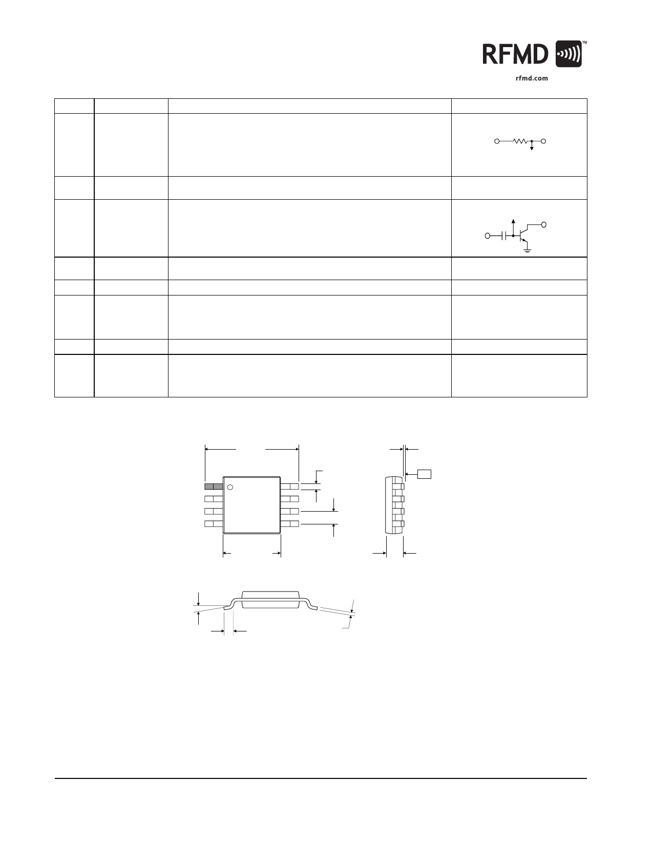
Pin Function Description
Interface Schematic
1
VCC1
Supply voltage for the LNA. External RF and IF bypassing is required.
The trace length between the pin and the bypass capacitors should be
minimized. The ground side of the bypass capacitors should connect
VCC1
150 Ω
VCC2
immediately to ground plane. This pin connects to pin 8 through a
BIAS
150Ω resistor. This allows for simple biasing of the collector at pin 6.
Refer to Application Schematics 1 and 3.
2
GND1
Ground connection. For best performance, keep traces physically short
and connect immediately to ground plane.
3
RF IN
RF input pin. This pin is internally DC-blocked and matched to 50Ω for
frequencies above 1GHz. When using below 1GHz, it is recommended
To bias circuits
that this pin be matched with series inductance to series-resonate out
LNA OUT
LNA IN
the internal blocking capacitor. Refer to Application Schematics 1 and
4
2.
4
GND2
Ground connection. For best performance, keep traces physically short
and connect immediately to ground plane.
5
NC
No connection. This pin is typically left unconnected or grounded.
6
RF OUT LNA Output pin. This pin is an open-collector output. It must be biased See pin 3.
to either VCC or pin 8 through a choke or matching inductor. This pin is
typically matched to 50Ω with a shunt bias/matching inductor and
series blocking/matching capacitor. Refer to application schematics.
7
NC
No connection. This pin is typically left unconnected or grounded.
8
VCC2
Optional power supply connection for biasing pin 6. This pin connects See pin 1.
to pin 1 through a 150Ω resistor. This allows for simple biasing of the
collector at pin 6. When used, this pin should be RF bypassed. Refer to
Application Schematics 1 and 3.
4-234
Rev B6 010612
Share Link: 