SL34118N Ver la hoja de datos (PDF) - System Logic Semiconductor
Número de pieza
componentes Descripción
Fabricante
SL34118N Datasheet PDF : 12 Pages
| |||
SL34118
recommended input signal is independent of the
volume control setting. The diode clamp on the
inputs limits the input swing, and therefore the
maximum negative output swing. This is the reason
for VRXOL and VTXOL specification being defined as
they are in the Electrical Characteristics. The output
impedance is <10 Ω until the output current limit
(typically 2.5 mA) is reached.
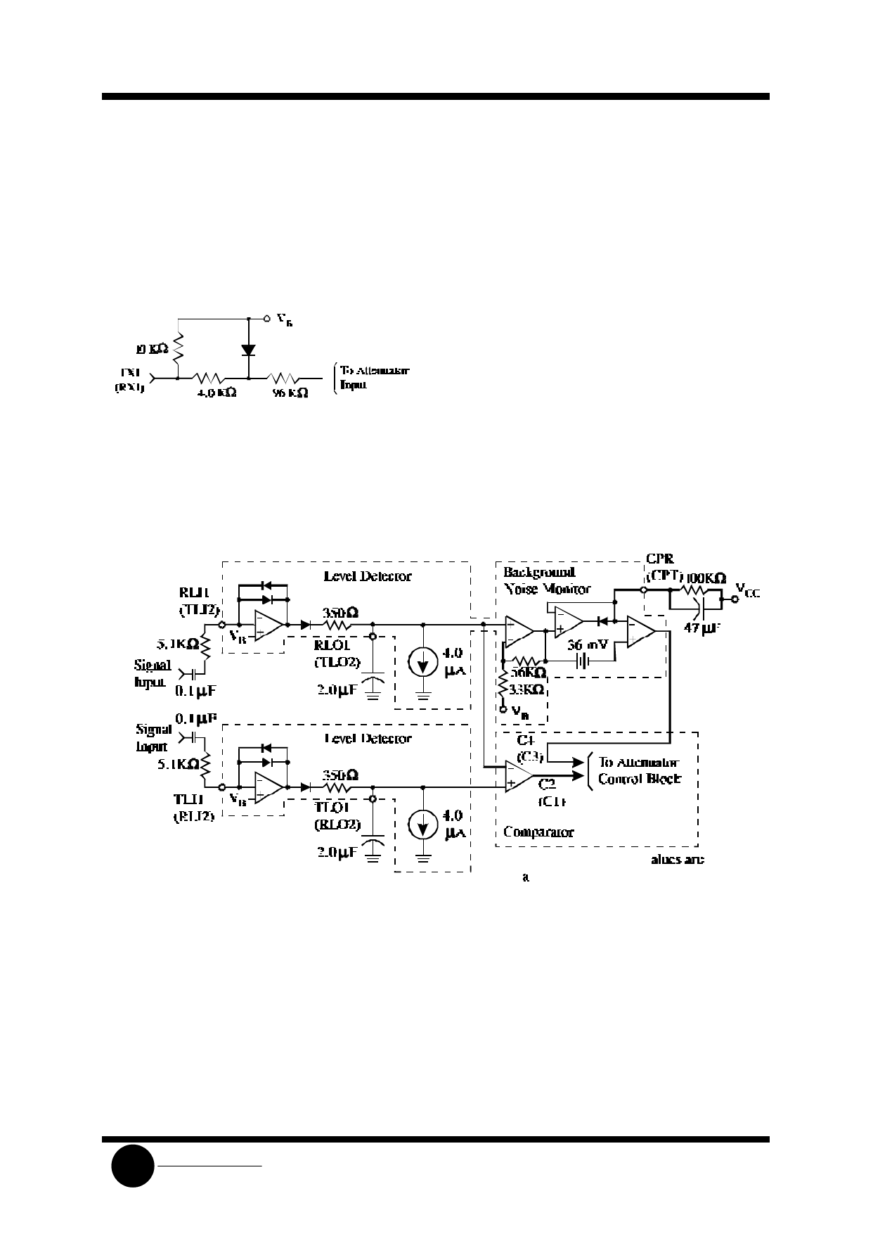
Figure 1. Attenuator Input Stage
the CT pin is at -240 millivolts with respect to VB, the
circuit is in the transmit mode (transmit attenuator is
at +6.0 dB). The circuit is in an idle mode when the CT
voltage is equal to VB, causing the attenuators’ gains
to be halfway between their fully on and fully off
positions (-20 dB each). Monitoring the CT voltage
(with respect to VB) is the most direct method of
monitoring the circuit’s mode.
The inputs to the Control Block are seven: 2 from
the comp arators operated by the level detectors, 2
from the background noise monitors, the volume
control, the dial-tone detector, and the AGC circuit.
These seven inputs are described below.
LEVEL DETECTORS
The attenuators are controlled by the single
output of the Control Block, which is measurable at
the CT pin (Pin 14). When the CT pin is at
+240 millivolts with respect to VB, the circuit is in the
receive mode (receive attenuator is at +6.0 dB). When
There are four level detectors - two on the receive
side and two on the transmit side. Refer to Figure
2 - the terms in parentheses form one system, and the
other terms form the second system
Figure 2. Level Detectors
Each level detector is a high gain amplifier with
back-to-back diodes in the feedback path, resulting in
non-linear gain, which permits operation over a wide
dynamic range of speech levels. The sensitivity of
each level detector is determined by the external
resistor and capacitor at each input (TLI1, TLI2, RLI1,
and RLI2). Each output charges an external capacitor
through a diode and limiting resistor, thus providing a
dc representation of the input ac signal
level. The outputs have a guick rise time (determined
by the capacitor and an internal 350 Ω resistor), and a
slow decay time set by an internal current source and
the capacitor. The capacitors on the four outputs
should have the same value (±10%) to prevent timing
problems.
Referring to Figure 8, on the receive side, one
level detector (RLI1) is at the receive input receiving
the same signal as at Tip and Ring, and
SLS
System Logic
Semiconductor
Share Link: 