M50LPW041K Ver la hoja de datos (PDF) - STMicroelectronics
Número de pieza
componentes Descripción
Fabricante
M50LPW041K Datasheet PDF : 37 Pages
| |||
M50LPW041
SIGNAL DESCRIPTIONS
There are two different bus interfaces available on
this part. The active interface is selected before
power-up or during Reset using the Interface Con-
figuration Pin, IC.
The signals for each interface are discussed in the
Low Pin Count (LPC) Signal Descriptions section
and the Address/Address Multiplexed (A/A Mux)
Signal Descriptions section below. The supply sig-
nals are discussed in the Supply Signal Descrip-
tions section below.
Low Pin Count (LPC) Signal Descriptions
For the Low Pin Count (LPC) Interface see Figure
1, Logic Diagram, and Table 1, Signal Names.
Input/Output Communications (LAD0-LAD3). All
Input and Output Communication with the memory
take place on these pins. Addresses and Data for
Bus Read and Bus Write operations are encoded
on these pins.
Input Communication Frame (LFRAME). The
Input Communication Frame (LFRAME) signals
the start of a bus operation. When Input Commu-
nication Frame is Low, VIL, on the rising edge of
the Clock a new bus operation is initiated. If Input
Communication Frame is Low, VIL, during a bus
operation then the operation is aborted. When In-
put Communication Frame is High, VIH, the cur-
rent bus operation is proceeding or the bus is idle.
Identification Inputs (ID0-ID3). The Identification
Inputs (ID0-ID3) allow to address up to 16
memories on a bus. The value on addresses A19-
A22 is compared to the hardware strapping on the
ID0-ID3 pins to select which memory is being
addressed, as shown in Table 2.
General Purpose Inputs (GPI0-GPI4). The Gener-
al Purpose Inputs can be used as digital inputs for
the CPU to read. The General Purpose Input Reg-
ister holds the values on these pins. The pins must
have stable data from before the start of the cycle
that reads the General Purpose Input Register un-
til after the cycle is complete. These pins must not
be left to float, they should be driven Low, VIL, or
High, VIH.
Interface Configuration (IC). The Interface Con-
figuration input selects whether the Low Pin Count
(LPC) or the Address/Address Multiplexed (A/A
Mux) Interface is used. The chosen interface must
be selected before power-up or during a Reset
and, thereafter, cannot be changed. The state of
the Interface Configuration, IC, should not be
changed during operation.
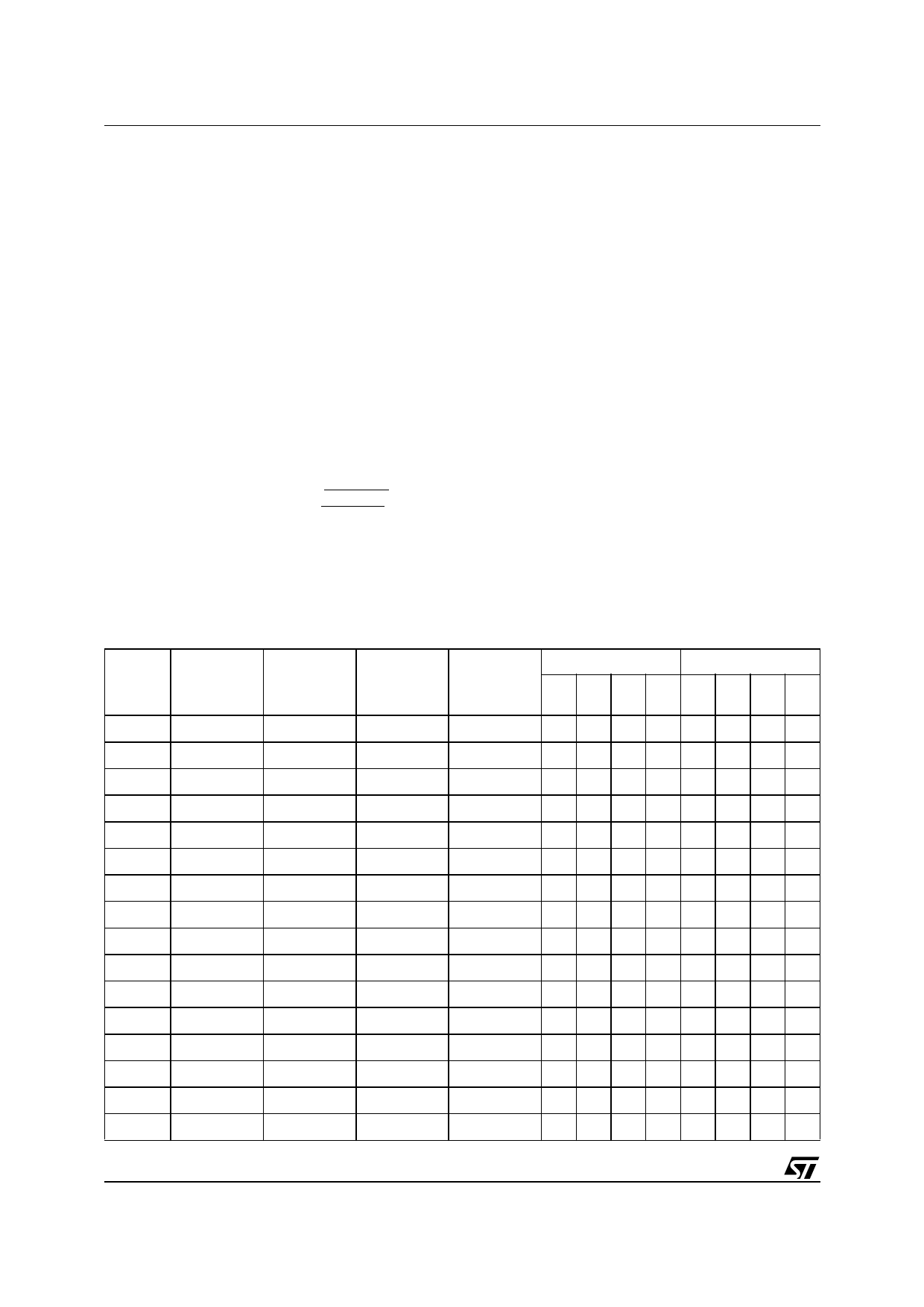
Table 2. Memory Identification Input Configuration
Top
Bottom
Memory
Number
ID2
ID2
ID1
ID0
AAAAAAAA
22 21 20 19 22 21 20 19
1 (Boot) VIL or floating VIL or floating VIL or floating VIL or floating 1 1 1 1 0 0 0 1
2
VIL or floating VIL or floating VIL or floating
VIH
11100000
3
VIL or floating VIL or floating
VIH
VIL or floating 1 1 0 1 0 0 1 1
4
VIL or floating VIL or floating
VIH
VIH
11000010
5
VIL or floating
VIH
VIL or floating VIL or floating 1 0 1 1 0 1 0 1
6
VIL or floating
VIH
VIL or floating
VIH
10100100
7
VIL or floating
VIH
VIH
VIL or floating 1 0 0 1 0 1 1 1
8
VIL or floating
VIH
VIH
VIH
10000110
9
VIH
VIL or floating VIL or floating VIL or floating 0 1 1 1 1 0 0 1
10
VIH
VIL or floating VIL or floating
VIH
01101000
11
VIH
VIL or floating
VIH
VIL or floating 0 1 0 1 1 0 1 1
12
VIH
VIL or floating
VIH
VIH
01001010
13
VIH
VIH
VIL or floating VIL or floating 0 0 1 1 1 1 0 1
14
VIH
VIH
VIL or floating
VIH
00101100
15
VIH
VIH
VIH
VIL or floating 0 0 0 1 1 1 1 1
16
VIH
VIH
VIH
VIH
00001110
4/37
Share Link: 