M62050 Ver la hoja de datos (PDF) - Renesas Electronics
Número de pieza
componentes Descripción
Fabricante
M62050 Datasheet PDF : 12 Pages
| |||
M62050P/FP
Operating Description
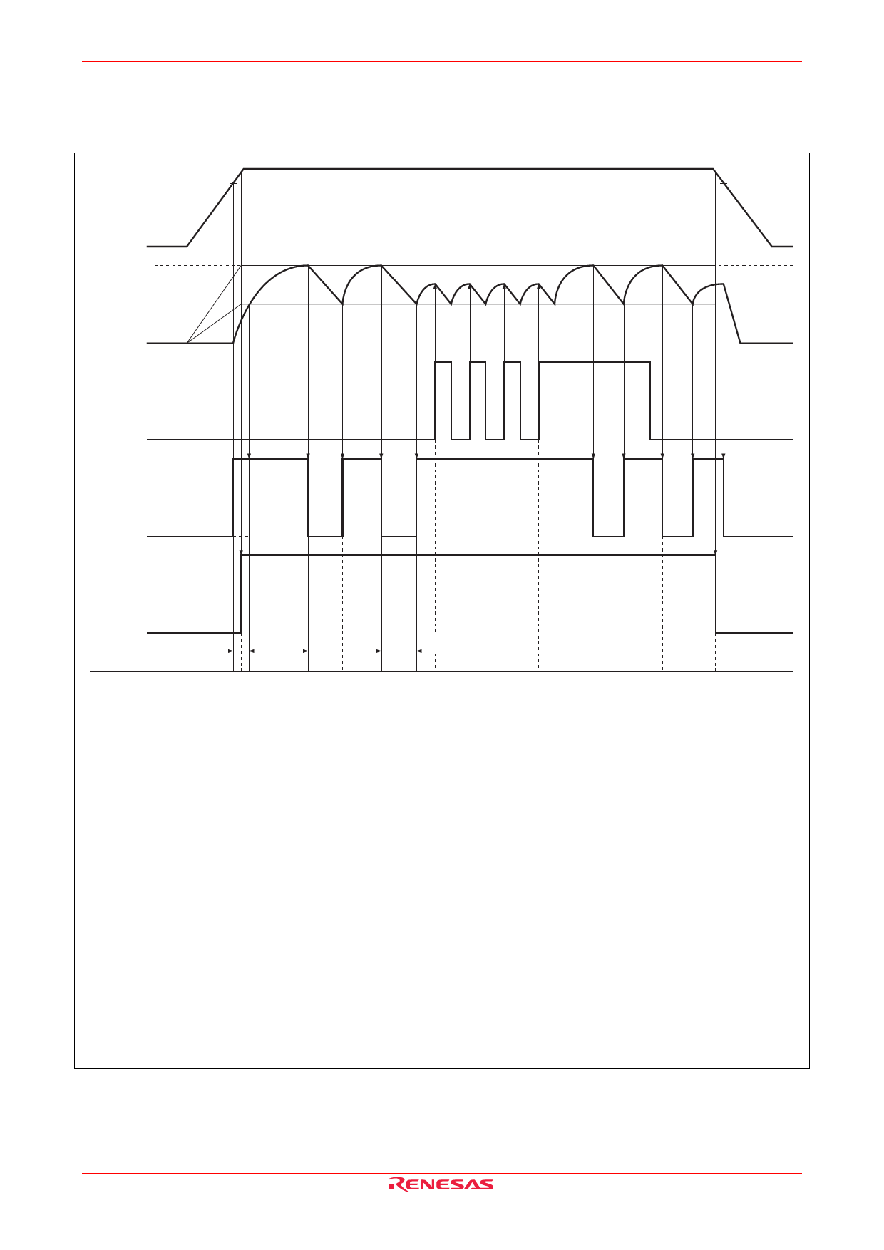
Timing Chart 1 (When the delay capacitor is not connected with Ct1 pin)
VCC
VTH1
VTH2(H)
VTH1(H)
0V
VTH3(H)
TC VTH3(L)
0V
VTH2(L)
VTH1(L)
WD
0V
RST1
Power ON
reset timer
0V
RST2
0V
tRST(1)
tWD
tRST(2)
(1)(2)(3)
(4) (5)
(6)
(7) (8)
(9) (10) (11)
(1): The VCC rises up to 0.8 V, then RST1 and RST2 generates low output, and rising up to 2.2 V(VTH1(H)), charge
of C1 begins.
(2): The VCC rises up to 2.5 V(VTH2(H)), then RST2 generates high.
(3), (4): The voltage at TC pin is 1.2 V(VTH3(L) = 2/5 VCC), then RST2 generates high, when 2.4 V(VTH3(H) = 4/5 VCC),
C1 is discharged and RST1 generates low.
(5): The voltage at TC pin falls to 1.2 V, then RST1 generates high unless normal clock signal is entered to WD
pin, RST1 repeats this operation.
(6), (7): Before the voltage at TC pin reaches 4 V, if normal clock signal is entered to WD pin, low RST1 is canceled.
(8), (9): In the case of entrance of abnormal signal input, as the waveform of TC pin repeats charge and discharge of
RST1 alternatively, the RST1 repeats high and low output operation.
(10): The VCC falls to 2.5 V(VTH2(L)), then RST2 generates low, this detective voltage has a 50 mV hysteresis.
(11): When VCC goes down to 2.2 V(VTH1(L)), the status of TC pin is switched to discharge. When the potentional at
TC pin is detected being VTH3(H) or VTH3(L), the status of RST1 becomes "low".
(This detective voltage has a 50 mV hysteresis.)
Terminology
tRST(1) : Time required for TC pin potential to rise from 0 V VTH3(L) when VCC is being applied.
tWD : Time required for TC pin potential to rise from VTH3(L) to VTH3(H).
tRST(2) : Time required for TC pin potential to go down from VTH3(H) to VTH3(L).
tdRST(1) : Time required for delay of charge with TC pin when VCC is impressed by connecting capacitor with Ct1 pin between GND.
Figure 1 Timing Chart 1
REJ03D0786-0200 Rev.2.00 Jun 15, 2007
Page 4 of 11
Share Link: 