MSK1461 Ver la hoja de datos (PDF) - M.S. Kennedy
Número de pieza
componentes Descripción
Fabricante
MSK1461 Datasheet PDF : 5 Pages
| |||
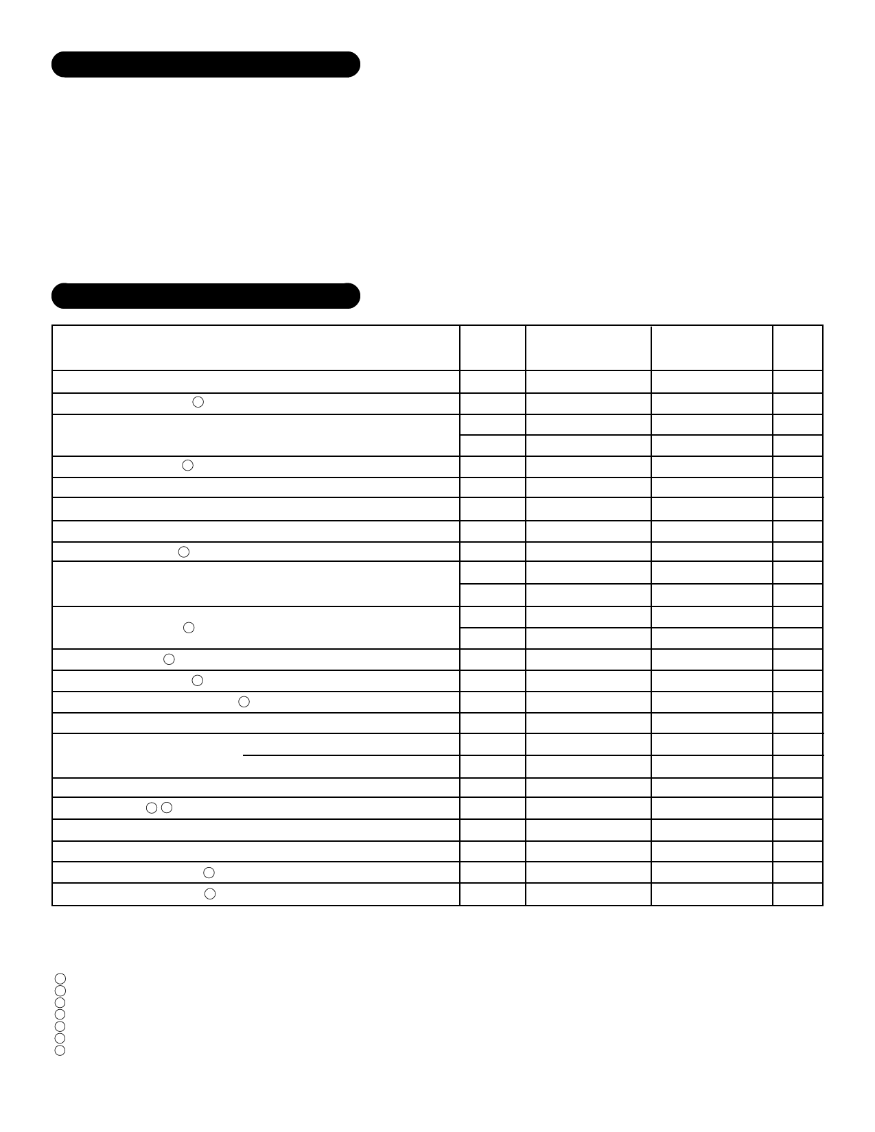
ABSOLUTE MAXIMUM RATINGS
±V Supply Voltage ±45V CC
○
○
○
○
○
○
○
○
○
○
○
○
○
○
○
○
IOUT
Output Current 800mA ○
○
○
○
○
○
○
○
○
○
○
○
○
○
○
VIN
Differential Input Voltage
○
○
○
○
○
○
○
○
○
○ ±25V
RTH
Thermal Resistance
○
○
○
○
○
○
○
○
○
○
○
○ 12°C/W
Junction to Case
(Output Devices Only)
TST Storage Temperature Range -65°C to +150°C
TLD
Lead Temperature Range
○
○
○
○
○
○
○
300°C
○
○
○
(10 Seconds)
TC Case Operating Temperature
(MSK 1461B)
-55°C to +125°C
○
○
○
○
○
○
○
○
○
○
(MSK 1461)
-40°C to 85°C
○
○
○
○
○
○
○
○
○
○
○
○
○
TJ
Junction Temperature
○
○
○
○
○
○
○
○
○
○
○ +175°C
ELECTRICAL SPECIFICATIONS
Parameter
Test Conditions
STATIC
Supply Voltage Range 3
Quiescent Current
VIN=0V
Thermal Resistance 3
INPUT
Input Offset Voltage
Input Offset Voltage Drift
Input Offset Adjust 3
Input Bias Current
Junction to Case
VIN=0V AV=-10V/V
Bal. Pins=N/C
RPOT=10KΩ to +VCC
VCM=0V
Either Input
Input Offset Current 3
VCM=0V
Input Impedance 3
Common Mode Range 3
F=DC
Common Mode Rejection Ratio 3
OUTPUT
F=10KHz VCM=±22V
Output Voltage Swing
Output Current, Peak
Settling Time 2 3
TRANSFER CHARACTERISTICS
RL=50Ω AV=-5V/V
RL=1KΩ
RL=33Ω AV=-5V/V TJ<175°C
0.1% 10V step
Slew Rate
Open Loop Voltage Gain 3
Gain Bandwidth Product 3
VOUT=±10V RL=1KΩ AV=-5V/V
RL=1KΩ F=100Hz
F=100KHz
Group A
Subgroup
MSK 1461B
Min. Typ. Max.
MSK 1461
Min. Typ. Max.
Units
-
±15 - ±45 ±15 - ±45 V
1
- ±19 ±25
- ±19 ±28 mA
2,3
- ±21 ±35
-
-
-
mA
-
-
11 12
-
11 15 °C/W
1
- ±1.0 ±5.0 - ±1.0 ±8.0 mV
2,3
- ±6.0 ±50
- ±10 - µV/°C
-
- ±8.0 -
- ±8.0 -
V
1
- ±10 ±300 - ±10 ±300 pA
2,3
- ±10 ±100 -
-
-
nA
-
- ±5.0 -
- ±5.0 -
pA
-
- ±5.0 -
-
-
-
nA
-
- 3x10¹² -
- 3x10¹² -
Ω
-
±22 ±24 -
±22 ±24 -
V
4
90 100 -
90 100 -
dB
4
±27 ±31 -
±27 ±31 -
V
4
±30 ±33 -
±30 ±33 -
V
4
±600 ±800 - ±600 ±800 -
mA
4
- 400 800
- 400 800 nS
4
200 500 -
200 500 -
V/µS
4
90 106 -
90 106 -
dB
4
800 1200 -
800 1200 -
MHz
NOTES:
1 RSC=0Ω and ±VCC=36VDC unless otherwise specified.
2 AV=-1, measured in false summing junction circuit.
3 Devices shall be capable of meeting the parameter, but need not be tested. Typical parameters are for reference only.
4 Industrial grade devices shall be tested to subgroups 1 and 4 unless otherwise specified.
5 Military grade devices ("B" suffix) shall be 100% tested to subgroups 1,2,3 and 4.
6 Subgroups 5 and 6 testing available upon request.
7 Subgroup 1,4 TC=+25°C
Subgroup 2,5 TJ=+125°C
Subgroup 3,6 TA=-55°C
2
Rev. B 8/00
Share Link: 