AD829SE/883B Ver la hoja de datos (PDF) - Analog Devices
Número de pieza
componentes Descripción
Fabricante
AD829SE/883B Datasheet PDF : 16 Pages
| |||
AD829
ABSOLUTE MAXIMUM RATINGS1
Supply Voltage . . . . . . . . . . . . . . . . . . . . . . . . . . . . . . . . ± 18 V
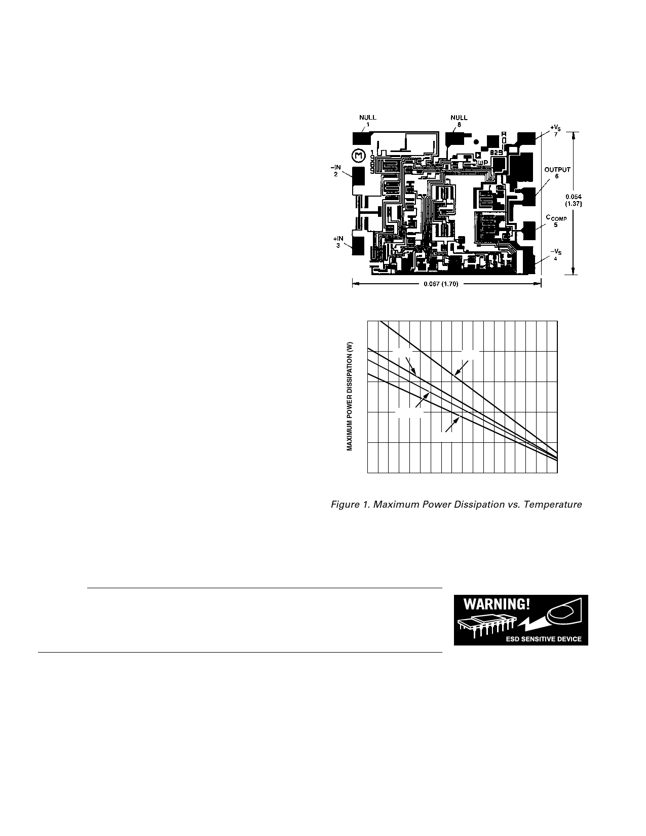
Internal Power Dissipation2
PDIP (N) . . . . . . . . . . . . . . . . . . . . . . . . . . . . . . . . . . . 1.3 W
SOIC (R) . . . . . . . . . . . . . . . . . . . . . . . . . . . . . . . . . . . 0.9 W
CERDIP (Q) . . . . . . . . . . . . . . . . . . . . . . . . . . . . . . . . 1.3 W
LCC (E) . . . . . . . . . . . . . . . . . . . . . . . . . . . . . . . . . . . 0.8 W
Input Voltage . . . . . . . . . . . . . . . . . . . . . . . . . . . . . . . . . . . . ± V
Differential Input Voltage3 . . . . . . . . . . . . . . . . . . . . . . . ± 6 V
Output Short Circuit Duration . . . . . . . . . . . . . . . . . Indefinite
Storage Temperature Range (Q, E) . . . . . . . . –65°C to +150°C
Storage Temperature Range (N, R) . . . . . . . . –65°C to +125°C
Operating Temperature Range
AD829J . . . . . . . . . . . . . . . . . . . . . . . . . . . . . . . 0°C to 70°C
AD829A . . . . . . . . . . . . . . . . . . . . . . . . . . . –40°C to +125°C
AD829S . . . . . . . . . . . . . . . . . . . . . . . . . . . –55°C to +125°C
Lead Temperature Range (Soldering 60 sec) . . . . . . . . . 300°C
NOTES
1 Stresses above those listed under Absolute Maximum Ratings may cause perma-
nent damage to the device. This is a stress rating only; the functional operation of
the device at these or any other conditions above those indicated in the operational
section of this specification is not implied. Exposure to absolute maximum rating
conditions for extended periods may affect device reliability.
2 Maximum internal power dissipation is specified so that TJ does not exceed
150°C at an ambient temperature of 25°C.
Thermal characteristics:
8-lead PDIP package: θJA = 100°C/W (derate at 8.7 mW/°C)
8-lead CERDIP package: θJA = 110°C/W (derate at 8.7 mW/°C)
20-lead LCC package: θJA = 77°C/W
8-lead SOIC package: θJA = 125°C/W (derate at 6 mW/°C).
3 If the differential voltage exceeds 6 V, external series protection resistors should
be added to limit the input current.
METALLIZATION PHOTO
Contact factory for latest dimensions.
Dimensions shown in inches and (mm).
SUBSTRATE CONNECTED TO +VS
2.5
2.0
PDIP
1.5
LCC
1.0
CERDIP
SOIC
0.5
0
–55 –45 –35 –25 –15 –5 5 15 25 35 45 55 65 75 85 95 105 115 125
AMBIENT TEMPERATURE (؇C)
Figure 1. Maximum Power Dissipation vs. Temperature
CAUTION
ESD (electrostatic discharge) sensitive device. Electrostatic charges as high as 4000 V readily
accumulate on the human body and test equipment and can discharge without detection. Although the
AD829 features proprietary ESD protection circuitry, permanent damage may occur on devices
subjected to high energy electrostatic discharges. Therefore, proper ESD precautions are recommended
to avoid performance degradation or loss of functionality.
–4–
REV. G
Share Link: 