VS32245 Ver la hoja de datos (PDF) - Vaishali Semiconductor
Número de pieza
componentes Descripción
Fabricante
VS32245 Datasheet PDF : 6 Pages
| |||
VS3245/VS32245
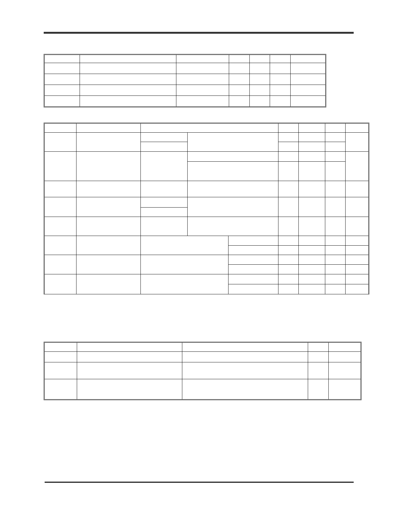
Table 5. Recommended Operating Conditions
Symbol
VCC
VIL
VIH
TA
Parameter
Power supply voltage
Low level input voltage
High level input voltage
Operating free-air temperature
Conditions
Min Typ Max Units
4.5
5.5 V
-0.5
0.8 V
2.0
5.5 V
-40
85
oC
Table 6. Electrical Characteristics Over Recommended Operating Free-air Temperature Range
Symbol
Parameter
VIK
Clamp Voltage
Control Input
Switch I/O
Test Conditions
VCC = Min, IIK = -18 mA
Min Typ(1) Max
-1.5
-1.5
VOH
Logic High Voltage Switch I/O
VIN = VCC = 5V, IOUT = -5µA
3.7
3.9
4.1
VCC = 4.3V, VN = 5V,
3.0
3.3
3.6
IOUT = -5µA
II
Input Leakage
Control Input VCC = Max, VI = VCC or GND
1
Current
|OFF|
Power OFF Leakage Control Input VCC = 0,
1
Current
Switch I/O
VI or VO = VCC or GND
|IOZ|
OFF State Leakage Switch I/O
VCC = Max, VI/O = VCC,
1
Current
/OE = VCC
IODL
Switch I/O Drive
VCC = Min, VIN = 0,
Current (Logic LOW) VOUT = 0.4V
VS3245
50
VS32245
IODH
Switch I/O Drive
VCC = Min, VIN = VCC,
Current (Logic HIGH) VOUT = 2.4V
VS3245
-50
VS32245
RON
Switch ON
Resistance(2)
VCC = Min, VIN = 0,
IOUT = 30mA
VS3245
VS32245
5
7
20
28
40
Notes:
1. Typical values are specified at VCC = 5.0V and TA = 25oC.
2. RON is measured by forcing specified current into the ‘output’ node of the switch with the ‘input’ node of the switch at the the
specified voltage
Units
V
V
µA
µA
µA
mA
mA
mA
mA
Ω
Ω
Table 7. Power Supply Characteristics Over Recommended Operating Free-air Temperature Range
Symbol
Parameter
Test Conditions (1)
Max Units
ICCQ
Quiescent Power Supply Current
VCC = Max, /OE = VCC or GND, f = 0
1
µA
∆ICC
QCCD
Power Supply Current per Input High
(Control Input) (2)
Dynamic Power Supply Current (3)
VCC = Max, VIN = 3.4V, f = 0
VCC = Max, Switch pins open,
Control Inputs toggling at 50% duty cycle
1.5 mA
0.25 mA/MHz
Notes:
1. For conditions shown as Min or Max, use the appropriate values per Recommended Operating Conditions.
2. Per TTL-driven control input. All other control inputs at GND. Switch I/O pins do not contribute to ∆ICC.
3. This parameter represents the average DC current resulting from the switching of internal nodes of the device at a given
frequency. The switch I/O pins make insignificant contribution to the dynamic power supply current of the device. This parameter
is guaranteed, but not production tested.
2001-04-12
Page 3
MDSS-0007-02
www.vaishali.com
Vaishali Semiconductor 747 Camden Avenue, Suite C Campbell CA 95008 Ph. 408.377.6060 Fax 408.377.6063
Share Link: 