MC145583DW Ver la hoja de datos (PDF) - LANSDALE Semiconductor Inc.
Número de pieza
componentes Descripción
Fabricante
MC145583DW
LANSDALE Semiconductor Inc.

MC145583DW Datasheet PDF : 7 Pages
| |||
LANSDALE Semiconductor, Inc.
ML145583
PIN DESCRIPTIONS
VCC
Digital Power Supply (Pin 27)
This digital supply pin is connected to the logic power supply. This
pin should have a not less than 0.33 µF capacitor GND.
GND
Ground (Pin 2)
Ground return pin is typically connected to the signal ground pin of
the EIA–232–E connector (Pin 7) as well as to the logic power sup-
ply ground.
VDD
Positive Power Supply (Pin 23)
This is the positive output of the on–chip voltage tripler and the
positive power supply input of the driver/receiver sections of the
device. This pin requires an external storage capacitor to filter the
50% duty cycle voltage generated by the charge pump.
VSS
Negative Power Supply (Pin 5)
This is the negative output of the on–chip voltage tripler/inverter
and the negative power supply input of the driver/ receiver sections
of the device. This pin requires an external storage capacitor to filter
the 50% duty cycle voltage generated by the charge pump.
the logic high level. During the standby mode, driver and receiver
output pins become high–impedance state. In this condition, supply
current ICC is below 5 µA (typ).
C5+, C5–, C2+, C2–, C1+, C1–
Voltage Tripler and Inverter (Pins 1, 3, 28, 26, 25, 24)
These are the connections to the internal voltage tripler and invert-
er, which generate the VDD and VSS voltages.
Rx1, Rx2, Rx3, Rx4, Rx5
Receive Data Inputs (Pins 7, 8, 9, 11, 13)
These are the EIA–232–E receive signal inputs. A voltage between
+ 3 and + 25 V is decoded as a space, and causes the corresponding
DO pin to swing to GND (0 V). A voltage between – 3 and – 25 V is
decoded as a mark, and causes the DO pin to swing up to VCC.
DO1, DO2, DO3, DO4, DO5
Data Outputs (Pins 22, 21, 20, 18, 16)
These are the receiver digital output pins, which swing from VCC
to GND. Output level of these pins is high impedance while in stand-
by mode.
DI1, DI2, DI3
Data Inputs (Pins 19, 17, 15)
These are the high impedance digital input pins to the drivers.
Input voltage levels on these pins must be betweenVCC and GND.
RIMON
Ring Monitor Circuit (Pin 4)
The Ring Monitor Circuit will convert the input level on Rx1 pin
at standby mode and output on the RIMON pin.
STB
Standby Mode (Pin 6)
The device enters the standby mode while this pin is connected to
Tx1, Tx2, Tx3
Transmit Data Output (Pins 10, 12, 14)
These are the EIA–232–E transmit signal output pins, which
swing toward VDD and VSS. A logic 1 at a DI input causes the cor-
responding Tx output to swing toward VSS. The actual levels and
slew rate achieved will depend on the output loading (RL/CL). The
minimum output impedance is 300 Ω when turned off.
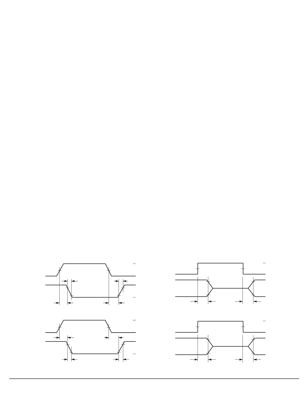
DRIVER
DI1 – DI3
(INPUT)
Tx1 – Tx3
(OUTPUT)
tDPHL
RECEIVER
Rx1 – Rx5
(INPUT)
DO1 – DO5
(OUTPUT)
50%
tf
90%
10%
tDPLH
50%
tRPHL
90%
10%
tf
SWITCHING CHARACTERISTICS
+3V
0V
tr
VOH
VOL
DRIVER
STB (INPUT)
Tx1 – Tx3
(OUTPUT)
tDAZ
+ 1.5 V
+5V
–5V
+3V
0V
tRPLH
VOH
VOL
tr
RECEIVER
STB (INPUT)
DO1 – DO5
(OUTPUT)
tRAZ
+ 1.5 V
90%
10%
HIGH Z
tDZA
+ 1.5 V
+ 3.3 V
0V
+ 5 V VOH
– 5 V VOL
HIGH Z
tRZA
+ 1.5 V
90%
+ 3.3 V
0V
VOH
10% VOL
Page 5 of 7
www.lansdale.com
Issue A
Share Link: