M95128-MN3 Ver la hoja de datos (PDF) - STMicroelectronics
Número de pieza
componentes Descripción
Fabricante
M95128-MN3 Datasheet PDF : 21 Pages
| |||
M95256, M95128
Table 4. Instruction Set
Instruc
tion
Description
Instruction
Format
WREN Set Write Enable Latch
0000 0110
WRDI Reset Write Enable Latch
0000 0100
RDSR Read Status Register
0000 0101
WRSR Write Status Register
0000 0001
READ Read Data from Memory Array 0000 0011
WRITE Write Data to Memory Array 0000 0010
Table 5. Status Register Format
b7
b0
SRWD X X X BP1 BP0 WEL WIP
Note: 1. SRWD, BP0 and BP1 are Read and write bits.
2. WEL and WIP are Read only bits.
As soon as the WREN or WRDI instruction is
received, the memory device first executes the
instruction, then enters a wait mode until the
device is deselected.
Read Status Register (RDSR)
The RDSR instruction allows the status register to
be read, and can be sent at any time, even during
a Write operation. Indeed, when a Write is in
progress, it is recommended that the value of the
Write-In-Progress (WIP) bit be checked. The value
in the WIP bit (whose position in the status register
is shown in Table 5) can be continuously polled,
before sending a new WRITE instruction, using
the timing shown in Figure 7. The Write-In-
Process (WIP) bit is read-only, and indicates
whether the memory is busy with a Write
operation. A ’1’ indicates that a write is in progress,
and a ’0’ that no write is in progress.
The Write Enable Latch (WEL) bit indicates the
status of the write enable latch. It, too, is read-only.
Its value can only be changed by one of the events
listed in the previous paragraph, or as a result of
executing WREN or WRDI instruction. It cannot be
changed using a WRSR instruction. A ’1’ indicates
that the latch is set (the forthcoming Write
instruction will be executed), and a ’0’ that it is
reset (and any forthcoming Write instructions will
be ignored).
The Block Protect (BP0 and BP1) bits indicate the
amount of the memory that is to be write-
protected. These two bits are non-volatile. They
are set using a WRSR instruction.
During a Write operation (whether it be to the
memory area or to the status register), all bits of
the status register remain valid, and can be read
using the RDSR instruction. However, during a
Write operation, the values of the non-volatile bits
(SRWD, BP0, BP1) become frozen at a constant
value. The updated value of these bits becomes
available when a new RDSR instruction is
executed, after completion of the write cycle. On
the other hand, the two read-only bits (WEL, WIP)
are dynamically updated during internal write
cycles. Using this facility, it is possible to poll the
WIP bit to detect the end of the internal write cycle.
Write Status Register (WRSR)
The format of the WRSR instruction is shown in
Figure 8. After the instruction and the eight bits of
the status register have been latched-in, the
internal Write cycle is triggered by the rising edge
of the S line. This must occur before the rising
edge of the 17th clock pulse (as indicated in Figure
14), otherwise the internal write sequence is not
performed.
The WRSR instruction is used for the following:
s to select the size of memory area that is to be
write-protected
s to select between SPM (Software Protected
Mode) and HPM (Hardware Protected Mode).
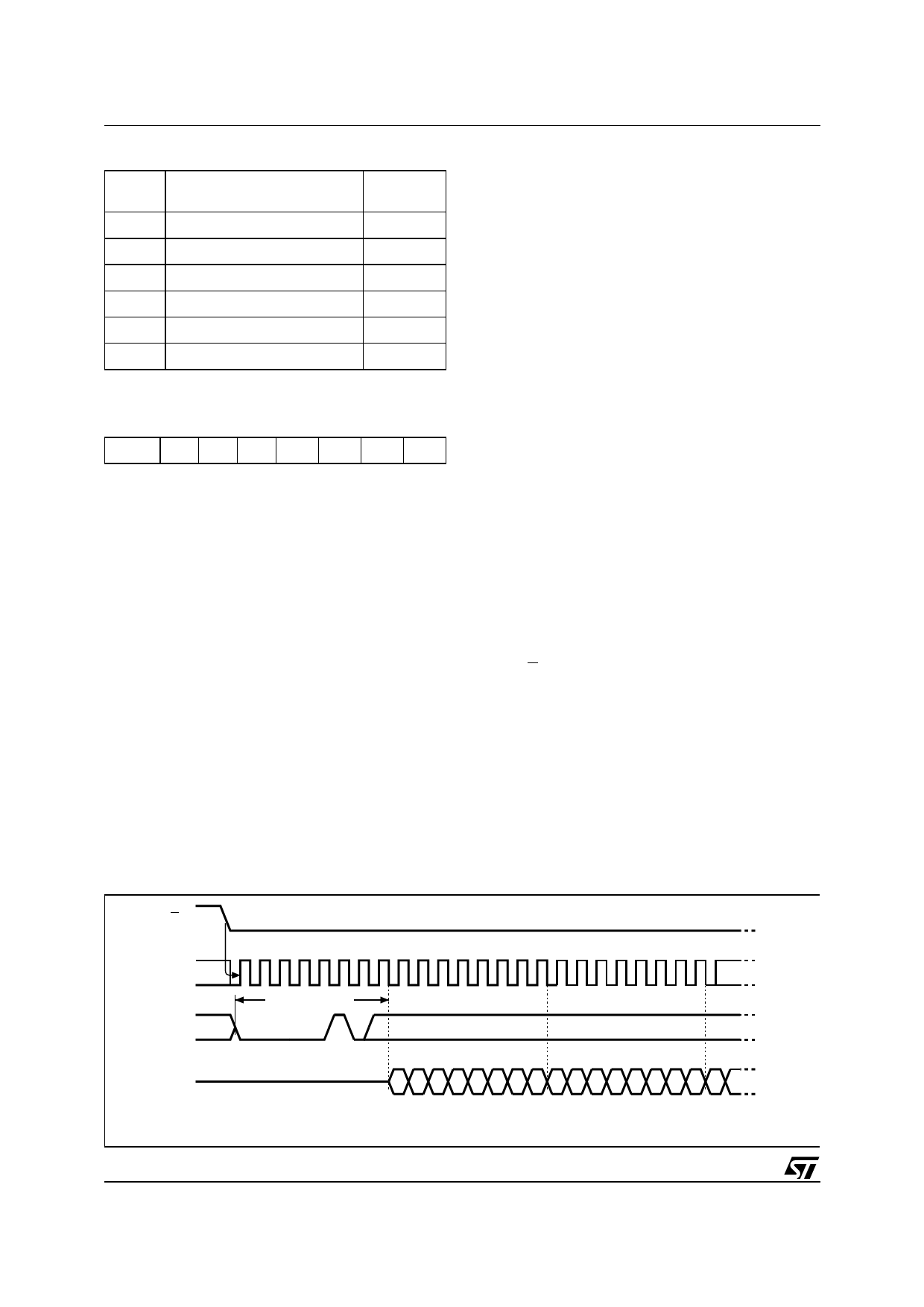
Figure 7. RDSR: Read Status Register Sequence
S
0 1 2 3 4 5 6 7 8 9 10 11 12 13 14 15
C
INSTRUCTION
D
STATUS REG. OUT
STATUS REG. OUT
HIGH IMPEDANCE
Q
76543210765432107
MSB
MSB
MSB
AI02031
6/21
Share Link: 