CMPWR101 Ver la hoja de datos (PDF) - ON Semiconductor
Número de pieza
componentes Descripción
Fabricante
CMPWR101 Datasheet PDF : 7 Pages
| |||
CMPWR101
SPECIFICATIONS
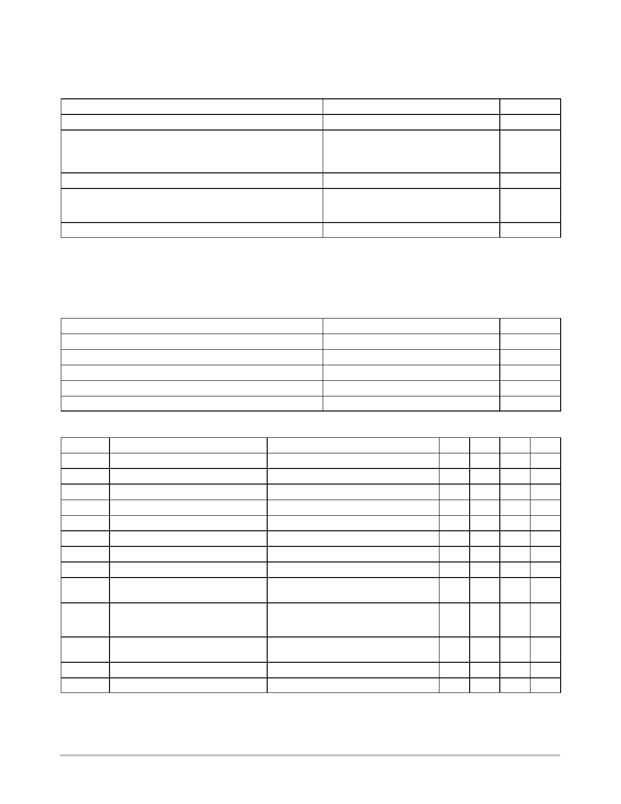
Table 2. ABSOLUTE MAXIMUM RATINGS
Parameter
Rating
Units
ESD Protection (HBM)
±2000
V
Pin Input Voltages
VCC
VAUX
DRIVE
Storage Temperature Range
V
[GND − 0.5] to +6.0
[GND − 0.5] to +4.0
[GND − 0.5] to [VCC + 0.5]
−40 to +150
°C
Operating Temperature Range
Ambient
Junction
°C
0 to +70
0 to +125
Power Dissipation (Note 1)
0.5
W
Stresses exceeding Maximum Ratings may damage the device. Maximum Ratings are stress ratings only. Functional operation above the
Recommended Operating Conditions is not implied. Extended exposure to stresses above the Recommended Operating Conditions may affect
device reliability.
1. The power rating is based on a printed circuit board heat spreading capability equivalent to 2 square inches of copper connected to the GND
pins. Typical multi−layer boards using power plane construction will provide this heat spreading ability without the need for additional
dedicated copper area. (Please consult with factory for thermal evaluation assistance).
Table 3. STANDARD OPERATING CONDITIONS
Parameter
VCC
VAUX
Ambient Operating Temperature Range
Load Current
CEXT
Rating
5.0 ±0.5
3.3 ±0.3
0 to +70
0 to 250
4.7 ±20%
Units
V
V
°C
mA
mF
Table 4. ELECTRICAL OPERATING CHARACTERISTICS (Note 2)
Symbol
Parameter
Conditions
Min Typ Max Units
VOUT
ILIM
VCCSEL
VCCDES
VCCHYST
VR LOAD
VR LINE
RSW
IRCC
IRAUX
Regulator Output Voltage
Regulator Current Limit
VCC Select Voltage
VCC Deselect Voltage
Hysteresis Voltage
Load Regulation
Line Regulation
VAUX Switch Resistance
VCC Reverse Leakage
VAUX Reverse Leakage
0 mA < ILOAD < 250 mA
Regulator Enabled
Regulator Disabled
(Note 3)
VCC = 5 V, 5 mA < ILOAD < 250 mA
ILOAD = 5 mA; 4.5 V < VCC < to 5.5 V
VCCDES > VCC, VAUX = 3.3 V
VAUX = 3.3 V, VCC = 0 V
VAUX = 0 V, VCC = 5 V
3.135 3.300 3.465 V
275
mA
4.30 4.45 V
3.90 4.10
V
0.20
V
20
mV
2
mV
0.25 0.40 W
2
50 mA
2
50
IGND
Ground Current
VCC < VCCDES, ILOAD = 0 mA
VCC > VCCSEL, ILOAD = 0 mA
VCC > VCCSEL, ILOAD = 250 mA
0.20 0.40 mA
0.60 1.00
0.70 1.20
IAUX
VAUX Supply Current
VAUX > VCC
VCC > VAUX
0.20 0.40 mA
0.02 0.10
ROH
DRIVE Pull−up Resistance
RPULLUP to VCC, VCC > VCCSEL
4.0 8.0 kW
ROL
DRIVE Pull−down Resistance
RPULLDOWN to GND, VCCDES > VCC
0.1 0.4 kW
2. Operating Characteristics are over Standard Operating Conditions unless otherwise specified.
3. The hysteresis defines the maximum level of acceptable disturbance on VCC during switching. It is recommended that the VCC source
impedance be kept below 0.25 W to ensure the switching disturbance remains below the hysteresis during select/deselect transitions. An
input capacitor may be required to help minimize the switching transient.
http://onsemi.com
3
Share Link: 