CMPWR101(2010) Ver la hoja de datos (PDF) - ON Semiconductor
Número de pieza
componentes Descripción
Fabricante
CMPWR101 Datasheet PDF : 12 Pages
| |||
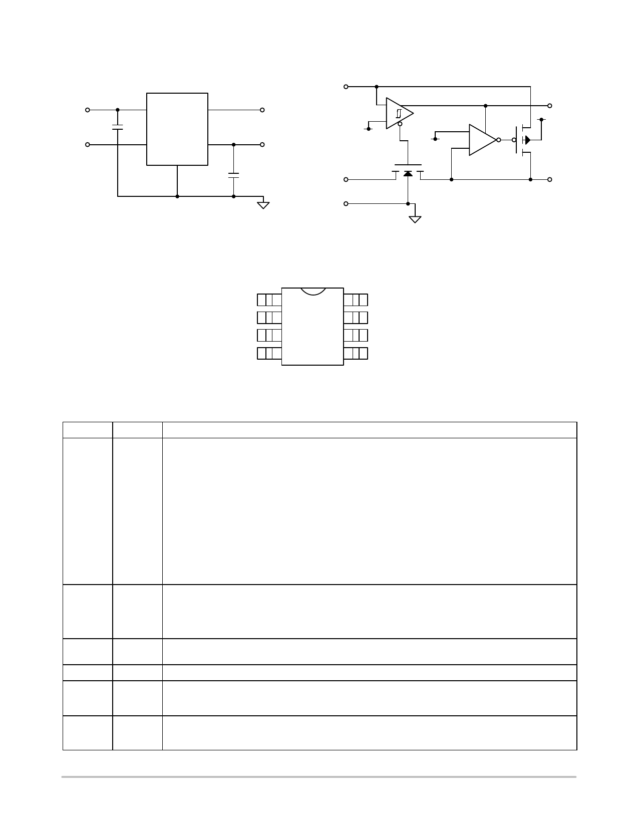
Typical Application Circuit
CMPWR101
Simplified Electrical Schematic
PIN(S)
1
2-3
4
5
6-7
8
PIN DESCRIPTIONS
NAME
VCC
VAUX
GND
DESCRIPTION
VCC is the power source for the internal regulator and is monitored continuously by an internal controller
circuit. Whenever VCC exceeds VCCSEL (4.25V typically), the internal regulator will be enabled and deliver
a fixed 3.3V at VOUT.
When VCC falls below VCCDES (4.10V typically), the regulator will be disabled. Internal loading on this pin is
typically 0.6mA when the regulator is enabled, which reduces to 0.1mA whenever the regulator is
disabled. If VCC falls below the voltage on the VAUX pin, the VCC loading will further reduce to only a few
microamperes. During a VCC power-up or power-down sequence, there will be an effective step increase
in VCC line current when the regulator is enabled/disabled. This line current transient will cause a voltage
disturbance at the VCC pin. The magnitude of the disturbance will be directly proportional to the effective
power supply source impedance being delivered to the VCC input.
A built-in hysteresis voltage of 150mV has been incorporated to minimize any chatter during supply
changeover. It is recommended that the power supply connected to the VCC input should have a source
resistance of less than 0.25Ω to minimize the event of chatter during the enabling/disabling of the
regulator.
If the VCC pin is within a few inches of the main input filter, a capacitor may not be necessary. Otherwise
an input filter capacitor in the range of 1µF to 10µF will help to lower the effective source impedance.
VAUX is the auxiliary power source. When selected, (VCC < VCCDES), the auxiliary supply is directly
connected to VOUT, via the low impedance (0.3Ω typically) fully integrated switch.
The internal loading on this pin is typically less than 10µA and will increase to 100µA if VCC falls below
the voltage on VAUX.
When VAUX = 0V, the VCCDES voltage is inhibited which prevents the regulator from being disabled.
GND is the negative reference for all voltages. The current that flows in the ground connection is very
low (typically 0.6mA) and has minimal variation over all load conditions.
NC
NC is an unconnected pin which is electrically isolated from the internal circuitry
VOUT
VOUT is the regulator output voltage connection used to power the load. An output capacitor of 4.7µF is
used to provide the necessary phase compensation, thereby preventing oscillation. The capacitor also
helps to minimize the peak output disturbance during power supply changeover.
DRIVE
DRIVE is a CMOS output logic signal (Active Low) referenced to the VCC supply. This output is taken low
whenever the internal regulator is not enabled. This output is intended only as a control signal for
external circuitry.
Rev. 3 | Page 2 of 12 | www.onsemi.com
Share Link: 