AD641-EB Ver la hoja de datos (PDF) - Analog Devices
Número de pieza
componentes Descripción
Fabricante
AD641-EB Datasheet PDF : 16 Pages
| |||
AD641
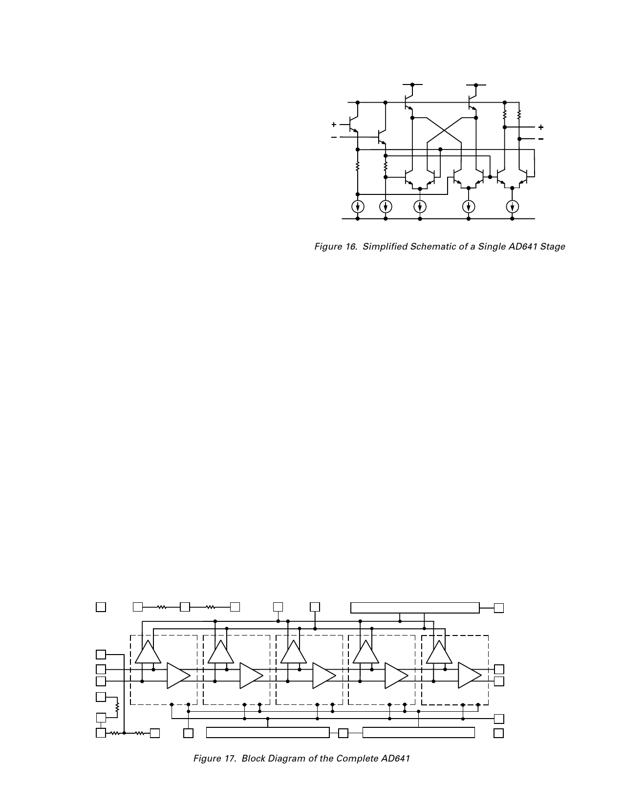
CIRCUIT DESCRIPTION
The AD641 uses five cascaded limiting amplifiers to approxi-
mate a logarithmic response to an input signal of wide dynamic
range and wide bandwidth. This type of logarithmic amplifier
has traditionally been assembled from several small scale ICs
and numerous external components. The performance of these
semidiscrete circuits is often unsatisfactory. In particular, the
logarithmic slope and intercept (see FUNDAMENTALS OF
LOGARITHMIC CONVERSION) are usually not very stable
in the presence of supply and temperature variations even after
laborious and expensive individual calibration. The AD641 em-
ploys high precision analog circuit techniques to ensure stability
of scaling over wide variations in supply voltage and tempera-
ture. Laser trimming, using ac stimuli and operating conditions
similar to those encountered in practice, provides fully cali-
brated logarithmic conversion.
Each of the amplifier/limiter stages in the AD641 has a small
signal voltage gain of 10 dB (×3.162) and a –3 dB bandwidth of
350 MHz. Fully differential direct coupling is used throughout.
This eliminates the many interstage coupling capacitors usually
required in ac applications, and simplifies low frequency signal
processing, for example, in audio and sonar systems. The AD641
is intended for use in demodulating applications. Each stage
incorporates a detector (a full-wave transconductance rectifier)
whose output current depends on the absolute value of its input
voltage.
Figure 16 is a simplified schematic of one stage of the AD641.
All transistors in the basic cell operate at near zero collector to
base voltage and low bias currents, resulting in low levels of
thermally induced distortion. These arise when power shifts
from one set of transistors to another during large input signals.
Rapid recovery is essential when a small signal immediately
follows a large one. This low power operation also contributes
significantly to the excellent long term calibration stability of the
AD641.
The complete AD641, shown in Figure 17, includes two bias
regulators. One determines the small signal gain of the ampli-
fier stages; the other determines the logarithmic slope. These
bias regulators maintain a high degree of stability in the re-
sulting function by compensating for potentially large uncer-
tainties in transistor parameters, temperature and supply
voltages. A third biasing block is used to accurately control
the logarithmic intercept.
COMMON
SIG
IN
LOG OUT
Q9
Q1
Q2
R1
85⍀
R2
85⍀
Q3 Q4
LOG COM
Q10
R3
75⍀
R4
75⍀
SIG
OUT
Q5 Q6
Q7 Q8
1.09mA 1.09mA
PTAT PTAT
565A
565A
–VS
2.18mA
PTAT
Figure 16. Simplified Schematic of a Single AD641 Stage
By summing the signals at the output of the detectors, a good
approximation to a logarithmic transfer function can be achieved.
The lower the stage gain, the more accurate the approximation,
but more stages are then needed to cover a given dynamic range.
The choice of 10 dB results in a theoretical periodic deviation or
ripple in the transfer function of ± 0.15 dB from the ideal re-
sponse when the input is either a dc voltage or a square wave.
The slope of the transfer function is unaffected by the input
waveform; however, the intercept and ripple are waveform de-
pendent (see EFFECT OF WAVEFORM ON INTERCEPT).
The input will usually be an amplitude modulated sinusoidal
carrier. In these circumstances the output is a fluctuating cur-
rent at twice the carrier frequency (because of the full wave
detection) whose average value is extracted by an external low
pass filter, which recovers a logarithmic measure of the base-
band signal.
Circuit Operation
With reference to Figure 16, the transconductance pair Q7, Q8
and load resistors R3 and R4 form a limiting amplifier having a
small signal gain of 10 dB, set by the tail current of nominally
2.18 mA at 27°C. This current is basically proportional to abso-
lute temperature (PTAT) but includes additional current to
compensate for finite beta and junction resistance. The limiting
output voltage is ± 180 mV at +27°C and is PTAT. Emitter
followers Q1 and Q2 raise the input resistance of the stage,
provide level shifting to introduce collector bias for the gain
stage and detectors, reduce offset drift by forming a thermally
balanced quad with Q7 and Q8 and generate the detector bias-
ing across resistors R1 and R2.
COM 18
RG1 1k⍀
17
RG0
16
1k⍀
RG2
15
LOG OUT LOG COM
14
13
INTERCEPT POSITIONING BIAS
12 +VS
ATN OUT 19
FULL-WAVE
DETECTOR
FULL-WAVE
DETECTOR
FULL-WAVE
DETECTOR
FULL-WAVE
DETECTOR
FULL-WAVE
DETECTOR
SIG +IN 20
SIG –IN 1
10dB
10dB
10dB
10dB
10dB
11 SIG +OUT
10 SIG –OUT
ATN LO 2
27⍀
ATN COM 3
30⍀
ATN COM 4
AMPLIFIER/LIMITER AMPLIFIER/LIMITER AMPLIFIER/LIMITER AMPLIFIER/LIMITER AMPLIFIER/LIMITER
270⍀
5
ATN IN
6
GAIN BIAS REGULATOR
7
SLOPE BIAS REGULATOR
BL1
–VS
Figure 17. Block Diagram of the Complete AD641
9 BL2
8 ITC
–6–
REV. C
Share Link: 