AD6411 Ver la hoja de datos (PDF) - Analog Devices
Número de pieza
componentes Descripción
Fabricante
AD6411 Datasheet PDF : 11 Pages
| |||
AD6411
L2
VCC
BPF1 LNA BPF2
VCC
S1
L1
PA
C1
SAW
C14
C13
LOAD
SYNTH
VCC
L3
C2 R2
R3 L4
TCI
V1
C3
C5
R1
C4
+
REF
+
DC RESTORE
BSW
TXDATA
X2
0...31
32/33
32/34
12/16
PFD
REFERENCE
REGULATOR #1
AD6411
CONTROLLER
INTERFACE
REGULATOR #2
DMOD DATA
C6
SFS
R4 VREF
C7
VBAT
Q1
VBAT
C8
Q2
C9
C10
R6
REF RSSI
C11
R5
VBAT
C12
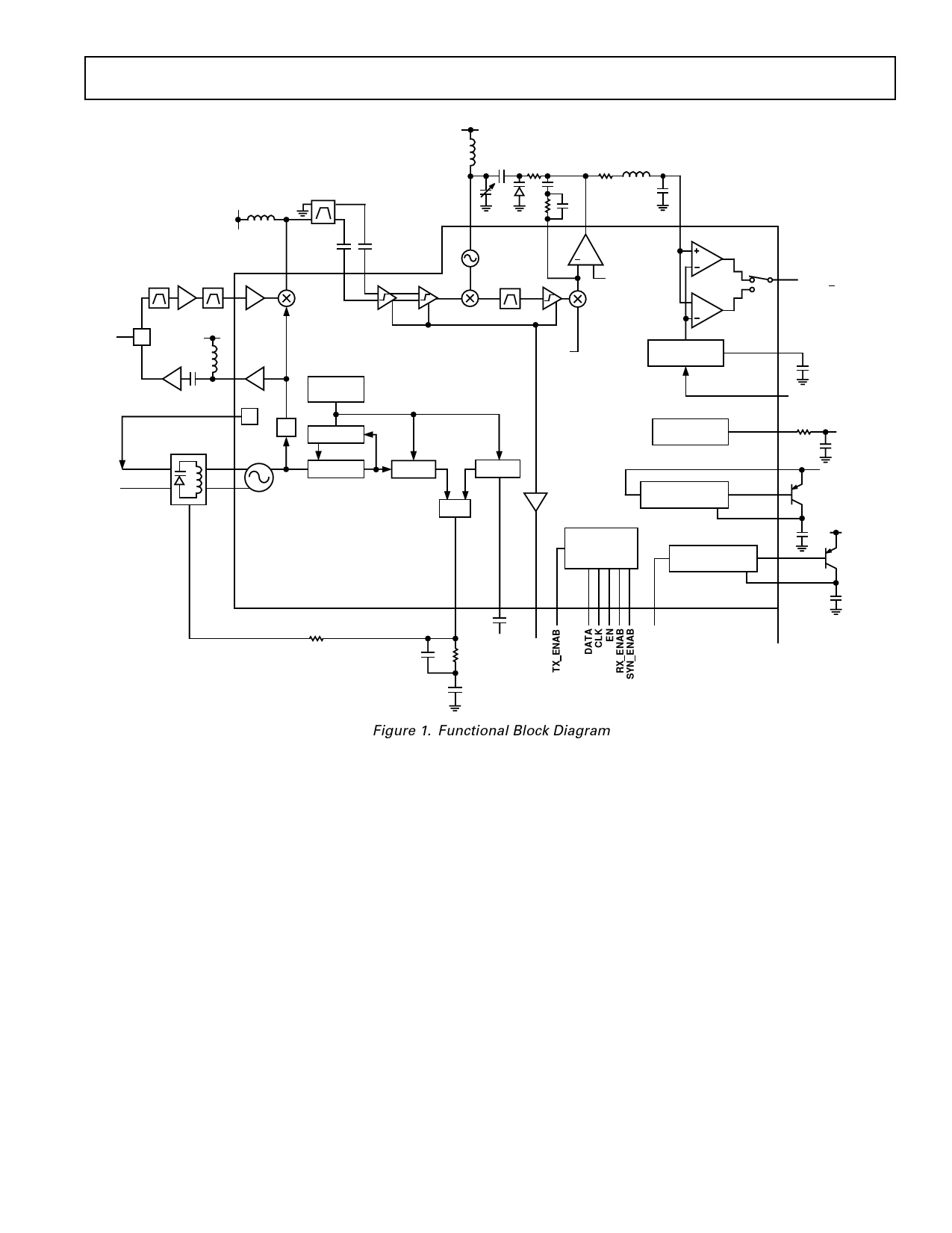
Figure 1. Functional Block Diagram
PRODUCT OVERVIEW
The AD6411 provides most of the active circuitry required to
realize a complete low power DECT transceiver.
Figure 1 shows the main sections of the AD6411. It consists, in
the receive path, of a UHF mixer and two-stage IF strip with
integrated demodulator and data slicer. The transmit path con-
sists of a VCO, frequency doubler and buffer amplifier.
Channel selection is performed by an on-chip PLL synthesizer.
All AD6411 operating modes can be controlled by parallel con-
trol inputs or the serial interface.
Receive Mixer
The UHF mixer is an improved Gilbert-cell design. The dy-
namic range at the input of the mixer is determined, at the up-
per end, by the maximum input signal level of –16 dBm in 50 Ω
at RFIN up to which the mixer remains linear and a valid RSSI
signal is provided and, at the lower end, by the noise level.
The local oscillator input of the receive mixer is internally pro-
vided by the LO, which is obtained by doubling the on-chip
VCO frequency.
The output of the mixer is single-ended. The nominal conver-
sion gain is specified for operation into a 110.592 MHz or
112.32 MHz SAW IF DECT bandpass filter. The power gain
of 17 dB is measured between the mixer input and the input of
this filter.
IF Circuits and Demodulator
Demodulation is achieved via a PLL. This is shown in detail in
Figure 2. An external manufacturing trim is required to achieve
the required level of frequency accuracy. The approach is to
adjust the capacitor TC1 (with the presence of an unmodulated
carrier) such that the dc level at Pin 3 (DEMOD_DATA) is
equal to the voltage on the external reference pin VREF.
Two demodulation modes are supported. In one mode any
frequency offset due to reference drift or frequency offsets on
the incoming carrier are propagated to the output (referred to as
“Normal” demodulation). The other method is to use a feature
of the DECT system that enables a secondary compensation
circuit to track out frequency offsets (“S-field sampling,” which
is enabled by the pin SFS—active high together with the con-
figuration bit SFM set over the serial interface).
REV. 0
–5–
Share Link: 