LTC1430 Ver la hoja de datos (PDF) - Linear Technology
Número de pieza
componentes Descripción
Fabricante
LTC1430 Datasheet PDF : 16 Pages
| |||
LTC1430
APPLICATIO S I FOR ATIO
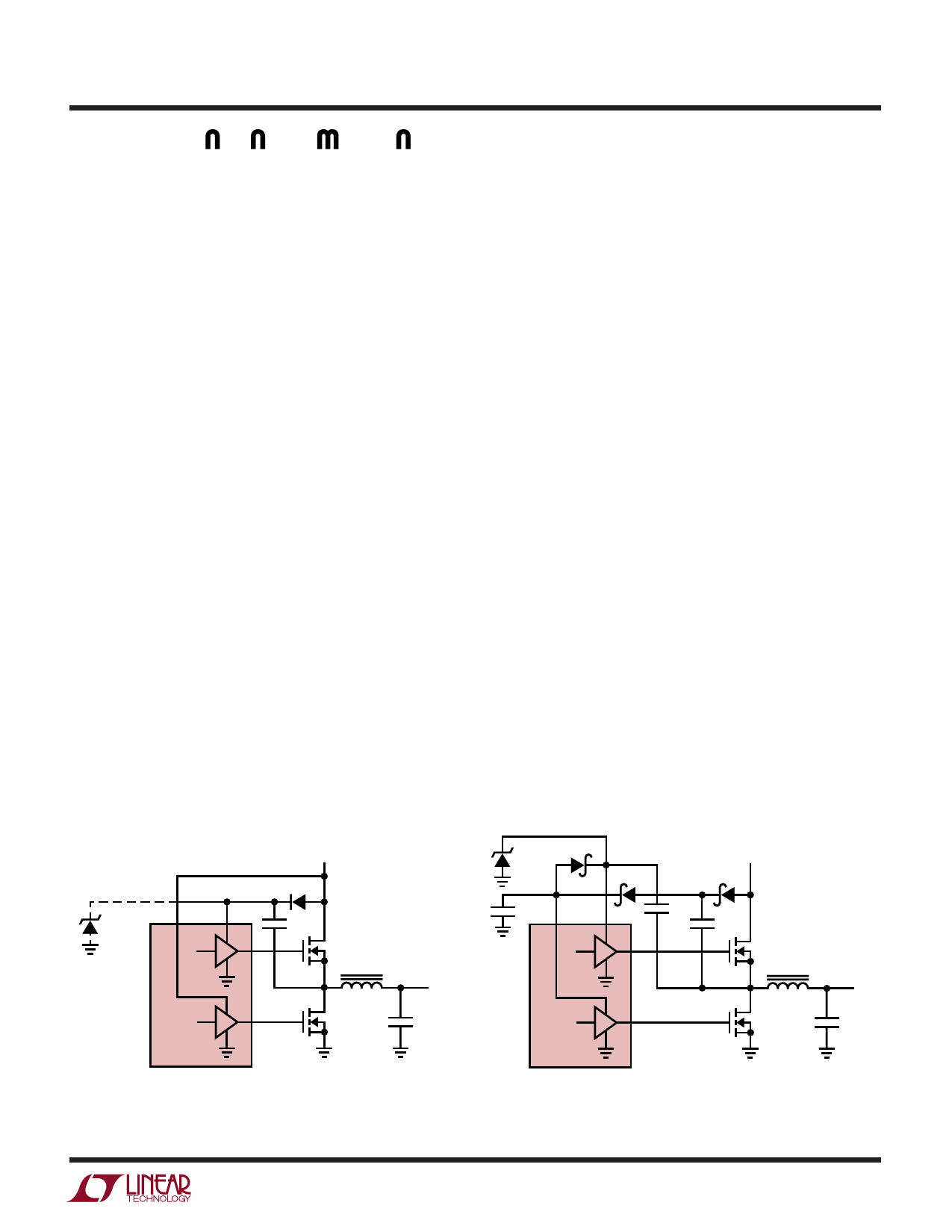
MOSFET Gate Drive
Gate drive for the top N-channel MOSFET M1 is supplied
from PVCC1. This supply must be above PVCC ( the main
power supply input) by at least one power MOSFET
VGS(ON) for efficient operation. An internal level shifter
allows PVCC1 to operate at voltages above VCC and PVCC,
up to 13V maximum. This higher voltage can be supplied
with a separate supply, or it can be generated using a
simple charge pump as shown in Figure 4. When using a
separate PVCC1 supply, the PVCC input may exhibit a large
inrush current if PVCC1 is present during power up. The
90% maximum duty cycle ensures that the charge pump
will always provide sufficient gate drive to M1. Gate drive
for the bottom MOSFET M2 is provided through PVCC2 for
16-lead devices or VCC/PVCC2 for 8-lead devices. PVCC2
can usually be driven directly from PVCC with 16-lead
parts, although it can also be charge pumped or connected
to an alternate supply if desired. The 8-lead parts require
an RC filter from PVCC to ensure proper operation; see
Input Supply Considerations.
EXTERNAL COMPONENT SELECTION
Power MOSFETs
Two N-channel power MOSFETs are required for most
LTC1430 circuits. These should be selected based prima-
rily on threshold and on-resistance considerations; ther-
mal dissipation is often a secondary concern in high
efficiency designs. Required MOSFET threshold should be
determined based on the available power supply voltages
and/or the complexity of the gate drive charge pump
scheme. In 5V input designs where an auxiliary 12V supply
is available to power PVCC1 and PVCC2, standard MOSFETs
with RDS(ON) specified at VGS = 5V or 6V can be used with
good results. The current drawn from this supply varies
with the MOSFETs used and the LTC1430’s operating
frequency, but is generally less than 50mA.
LTC1430 designs that use a doubler charge pump to
generate gate drive for M1 and run from PVCC voltages
below 7V cannot provide enough gate drive voltage to fully
enhance standard power MOSFETs. When run from 5V, a
doubler circuit may work with standard MOSFETs, but the
MOSFET RON may be quite high, raising the dissipation in
the FETs and costing efficiency. Logic level FETs are a
better choice for 5V PVCC systems; they can be fully
enhanced with a doubler charge pump and will operate at
maximum efficiency. Doubler designs running from PVCC
voltages near 4V will begin to run into efficiency problems
even with logic level FETs; such designs should be built
with tripler charge pumps (see Figure 5) or with newer,
super low threshold MOSFETs. Note that doubler charge
pump designs running from more than 7V and all tripler
charge pump designs should include a zener clamp diode
DZ at PVCC1 to prevent transients from exceeding the
absolute maximum rating at that pin.
OPTIONAL
USE FOR PVCC ≥ 7V
DZ
12V
1N5242
PVCC2
PVCC
1N4148
PVCC1
G1
0.1µF
M1
L1
G2
M2
VOUT
+
COUT
LTC1430
LTC1430 • F04
Figure 4. Doubling Charge Pump
DZ
12V
1N5242
1N5817
1N5817
PVCC
1N5817
10µF
PVCC2
PVCC1
G1
G2
0.1µF
0.1µF
M1
L1
M2
VOUT
+
COUT
LTC1430
LTC1430 • F05
Figure 5. Tripling Charge Pump
7
Share Link: 