MR82510 Ver la hoja de datos (PDF) - Intel
Número de pieza
componentes Descripción
Fabricante
MR82510 Datasheet PDF : 40 Pages
| |||
M82510
GENERAL DESCRIPTION
The M82510 can be functionally divided into seven
major blocks (See Fig 1) Bus Interface Unit Timing
Unit Modem Module Tx FIFO Rx FIFO Tx Ma-
chine and Rx Machine Six of these blocks (all ex-
cept Bus Interface Unit) can generate block inter-
rupts Three of these blocks can generate second-
level interrupts which reflect errors status within the
block (Receive Machine Timing Unit and the Mo-
dem Module)
The Bus interface unit allows the M82510 to inter-
face with the rest of the system It controls access to
device registers as well as generation of interrupts
to the external world The FIFOs buffer the CPU
from the Serial Machines and reduce the interrupt
overhead normally required for serial operations
The threshold (level of occupancy in the FIFO which
will generate an interrupt) is programmable for each
FIFO The timing unit controls generation of the sys-
tem clock through either its on-chip crystal oscillator
or an externally generated clock It also provides two
Baud Rate Generators Timers with various options
and modes to support serial communication
Its register set can be used in 8250A 16450 com-
patibility or High Performance modes The 8250A
16450 mode is the default wake-up mode in which
only the 8250A 16450 compatible registers are ac-
cessible The remaining registers are default config-
ured to support 8250A 16450 emulation
Software Interface
FUNCTIONAL DESCRIPTION
CPU Interface
The M82510 has a simple demultiplexed Bus Inter-
face which consists of a bidirectional three-state
eight-bit data bus and a three-bit address bus An
Interrupt pin along with the Read Write and Chip
Select are the remaining signals used to interface
with the CPU The three address lines along with the
Bank Pointer register are used to select the regis-
ters The M82510 is designed to interface to all Intel
microprocessor and microcontroller families Like
most other I O based peripherals it is programmed
through its registers to support a variety of functions
271072 – 3
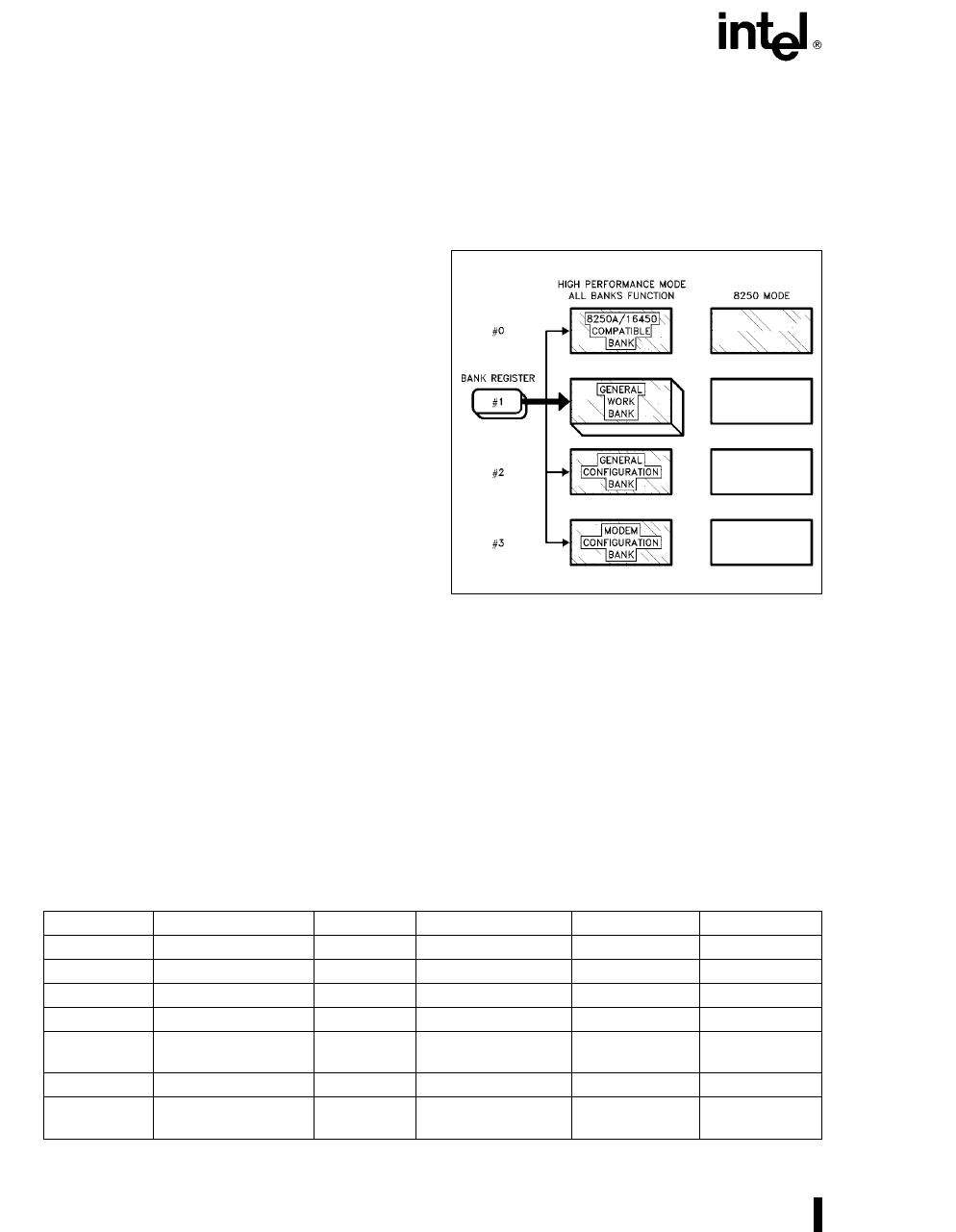
Figure 3 M82510 Register Architecture
The M82510 is configured and controlled through its
35 registers which are divided into four banks Only
one bank is accessible at any one time The bank
switching is done by changing the contents of the
bank pointer (GIR BANK – BANK0 BANK1) The
banks are logically grouped into 8250A 16450 com-
patible (0) General Work Bank (1) General Configu-
ration (2) and Modem Configuration (3) The
8250A 16450 compatible bank (Bank 0) is the de-
fault bank upon power up
The M82510 registers can be categorized under the
following
FIFO
MODEM
RX
TX
TIMER
DEVICE
8250
Table 2 M82510 Register Block Functions
Status
FLR
MSR
RST RXF
LSR
TMST
GSR GIR
LSR MSR GIR
Enable
MIE
RIE
LSR
TMIE
GER
GER
Configuration
FMD
PMD
RMD
TMD
CLCF
BACF BBCF
IMD
LCR MCR
Command
MCR
RCM
TCM
TMCR
ICM
MCR
Data
RXD RXF
TXD TXF
BBL BBH
BAL BAH
TXD RXD
BAL BAH
4
Share Link: 