VN16218 Ver la hoja de datos (PDF) - Vaishali Semiconductor
Número de pieza
componentes Descripción
Fabricante
VN16218 Datasheet PDF : 11 Pages
| |||
VN16218
Advance Information
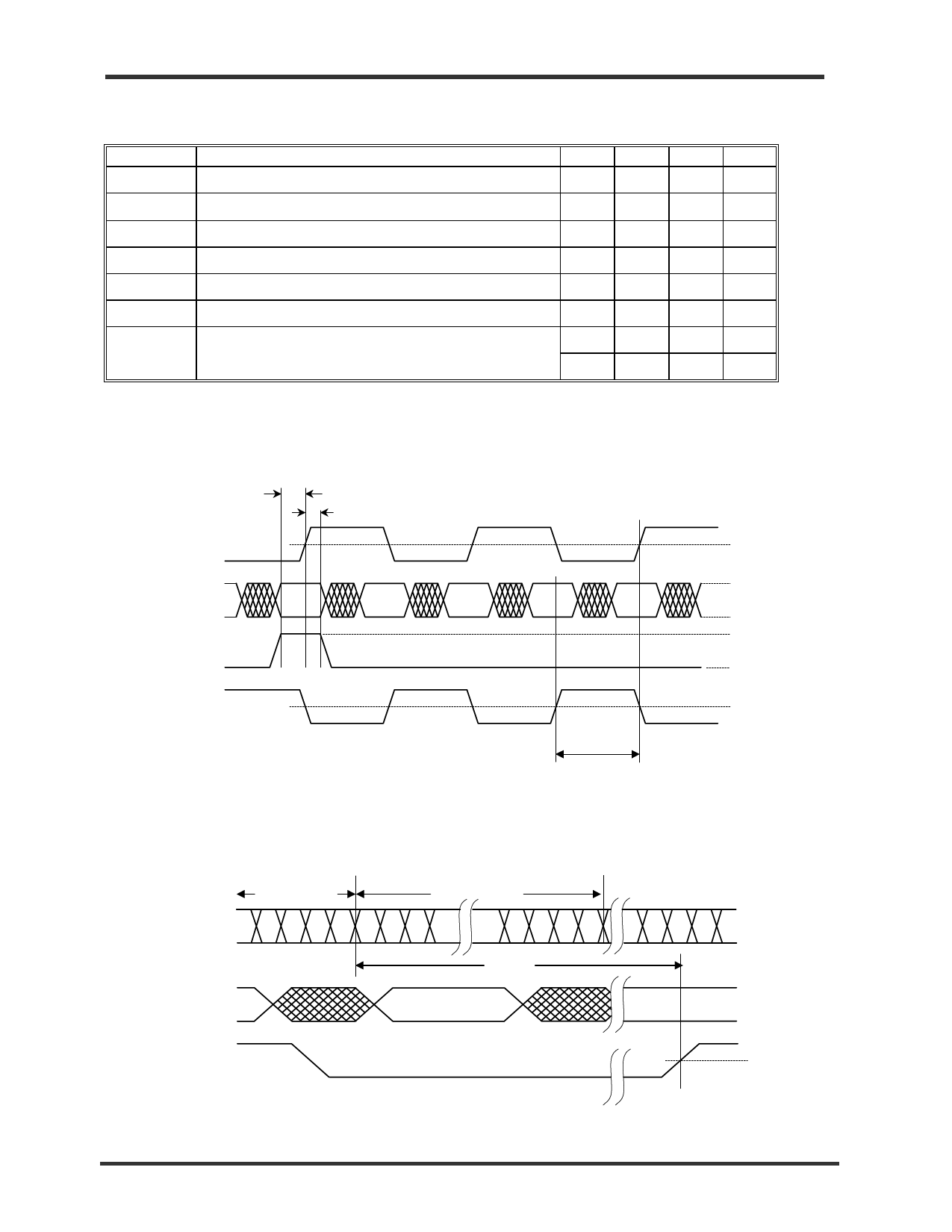
Table 12. Receiver Timing Characteristics
TA = 0°C to +70°C, Vcc = 3.15 V to 3.45 V
Symbol
Parameter
b_sync[1]
Bit Sync Time
Min. Typ. Max. Unit
2500 bits
f_lock
Frequency Lock at Powerup
500 µs
tSETUP
Data Setup Before Rising Edge of RBC,RBCN
2.5
nsec
tHOLD
Data Hold After Rising Edge of RBC,RBCN
1.5
nsec
tDUTY
RBC,RBCN Duty Cycle
40
60
%
tA-B
T_rxlat[2]
RBC,RBCN Skew
Receiver Latency
7.5
8.5 nsec
22.4
nsec
28.0
bits
Notes:
1. This is the recovery for input phase jumps.
2. The receiver latency as shown in Figure 8, is defined as the time between receiving the first serial bit of a parallel
data word (defined as the first edge of the first serial bit) and the clocking out of that parallel word (defined by the
rising edge of the receive byte clock, either RBC or RBCN).
tSETUP
RBC
tHOLD
1.4 V
R19:0
COM_DET
RBCN
K28.5
DATA
DATA
DATA
DATA
tA-B
2.0 V
0.8 V
2.0 V
0.8 V
1.4 V
Figure 7. Receiver Section Timing
DIN±
DATA BYTE C
DATA BYTE D
R15 R16 R17 R18 R19 R0 R1 R2
R16 R17 R18 R19
R19:0
t_rxlat
DATA BYTE A
R2 R3 R4 R5
DATA BYTE D
RBC/RBCN
1.4 V
Figure 8. Receiver Latency
2001-11-09
Page 9
MDSN-0003-00
www.vaishali.com
Vaishali Semiconductor 747 Camden Avenue, Suite C Campbell CA 95008 Ph. 408.377.6060 Fax 408.377.6063
Share Link: 