TDA8547TS Ver la hoja de datos (PDF) - NXP Semiconductors.
NĂșmero de pieza
componentes DescripciĂłn
Fabricante
TDA8547TS Datasheet PDF : 21 Pages
| |||
NXP Semiconductors
2 Ă 0.7 W BTL audio amplifier with
output channel switching
Product specification
TDA8547TS
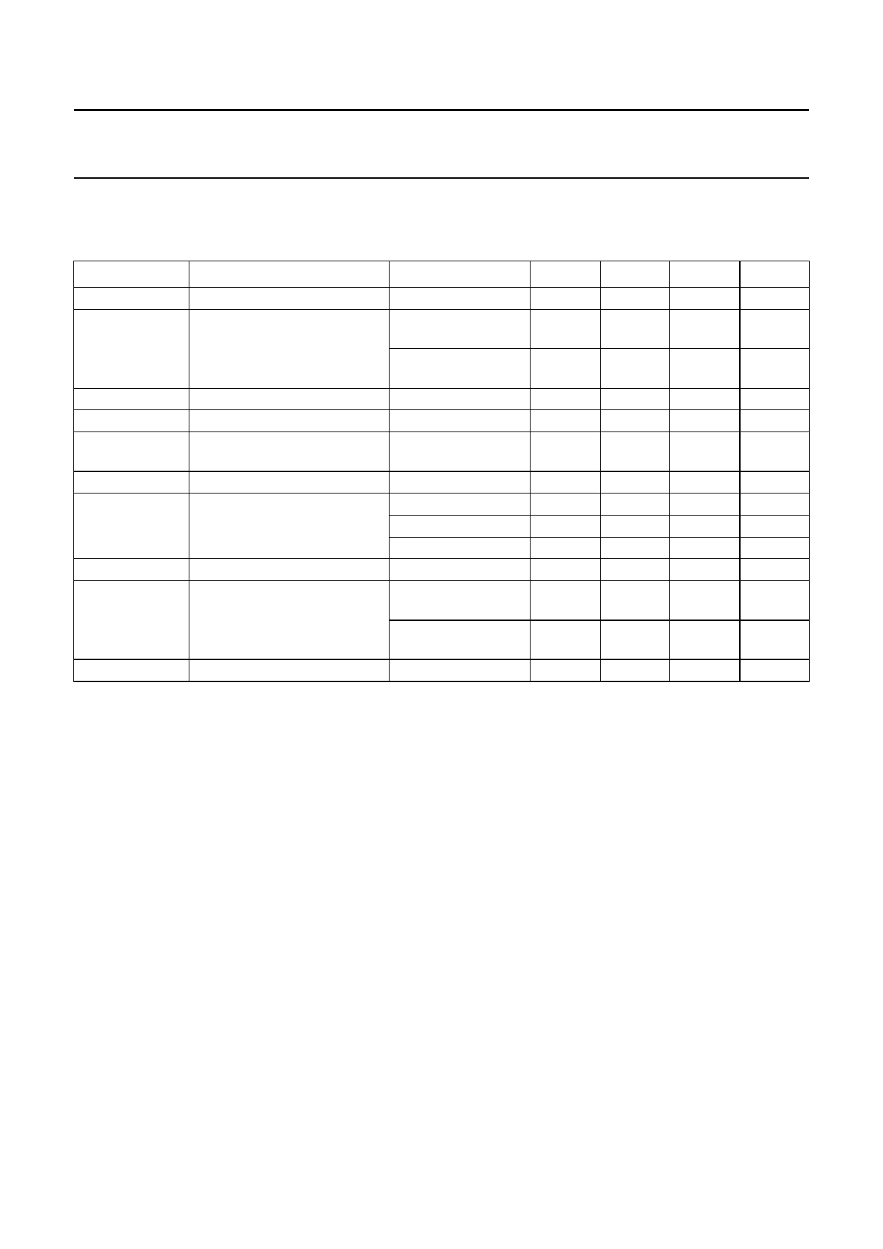
DC CHARACTERISTICS
VCC = 5 V; Tamb = 25 °C; RL = 8 Ω; VMODE = 0 V; gain = 20 dB; measured in BTL application circuit Fig.4; unless
otherwise specified.
SYMBOL
VCC
Iq
PARAMETER
supply voltage
quiescent current
Istb
standby current
VO
DC output voltage
âȘVOUT+ â VOUTââȘ differential output voltage
offset
IIN+, IINâ
input bias current
VMODE
input voltage MODE pin
IMODE
VSELECT
input current MODE pin
input voltage SELECT pin
ISELECT
input current SELECT pin
CONDITIONS
operating
BTL 2 channels;
note 1
BTL 1 channel;
note 1
VMODE = VCC
note 2
MIN.
2.2
â
TYP.
5
15
MAX.
18
22
UNIT
V
mA
â
8
12
mA
â
â
10
ÎŒA
â
2.2
â
V
â
â
50
mV
â
â
operating
0
â
mute
1.5
â
standby
0 V < VMODE < VCC
VCC â 0.5 â
â
â
channel 1 = standby; 0
â
channel 2 = on
channel 1 = on;
VCC â 1 â
channel 2 = standby
VSELECT = 0 V
â
â
500
nA
0.5
V
VCC â 1.5 V
VCC
V
20
ÎŒA
1
V
VCC
V
100
ÎŒA
Notes
1. Measured with RL = â. With a load connected at the outputs the quiescent current will increase, the maximum of this
increase being equal to the DC output offset voltage divided by RL.
2. The DC output voltage with respect to ground is approximately 0.5VCC.
1998 Apr 01
7
Share Link: 