CS5201-1 Ver la hoja de datos (PDF) - Cherry semiconductor
Número de pieza
componentes Descripción
Fabricante
CS5201-1 Datasheet PDF : 7 Pages
| |||
Absolute Maximum Ratings
Supply Voltage, VCC . . . . . . . . . . . . . . . . . . . . . . . . . . . . . . . . . . . . . . . . . . . . . . . . . . . . . . . . . . . . . . . . . . . . . . . . . . . . . . . . . . . .7V
Operating Temperature Range . . . . . . . . . . . . . . . . . . . . . . . . . . . . . . . . . . . . . . . . . . . . . . . . . . . . . . . . . . . . . . . . .-40¡C to 70¡C
Junction Temperature . . . . . . . . . . . . . . . . . . . . . . . . . . . . . . . . . . . . . . . . . . . . . . . . . . . . . . . . . . . . . . . . . . . . . . . . . . . . . . . .150¡C
Storage Temperature Range . . . . . . . . . . . . . . . . . . . . . . . . . . . . . . . . . . . . . . . . . . . . . . . . . . . . . . . . . . . . . . . . . . .-60¡C to 150¡C
Lead Temperature Soldering
Wave Solder (through hole styles only) . . . . . . . . . . . . . . . . . . . . . . . . . . . . . . . . . . . . . . . . . . . .10 sec. max, 260¡C peak
Reflow (SMD styles only) . . . . . . . . . . . . . . . . . . . . . . . . . . . . . . . . . . . . . . . . . . . . .60 sec. max above 183¡C, 230¡C peak
ESD Damage Threshold (Human Body Model) . . . . . . . . . . . . . . . . . . . . . . . . . . . . . . . . . . . . . . . . . . . . . . . . . . . . . . . . . . .2kV
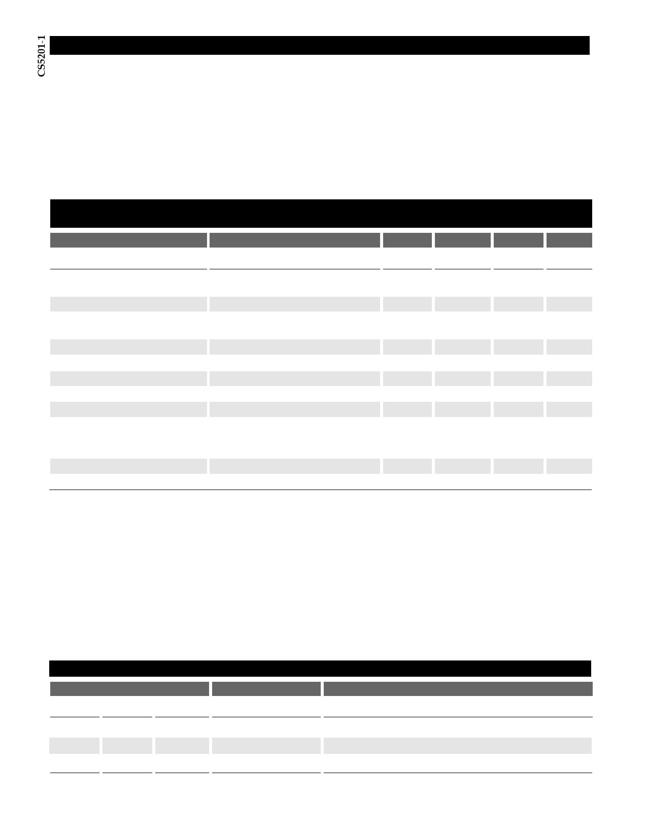
Electrical Characteristics: CIN = 10µF, COUT = 22µF Tantalum, VOUT + VDROPOUT < VIN < 7V, 0¡C ² TA ² 70¡C, TJ ² +150¡C,
unless otherwise specified, Ifull load = 1A.
PARAMETER
TEST CONDITIONS
MIN
TYP
MAX
UNIT
s Adjustable Output Voltage
Reference Voltage
(Notes 1 and 2)
Line Regulation
Load Regulation
(Notes 1 and 2)
VINÐVOUT=1.5V; VAdj = 0V
10mA²IOUT²1A
1.5V²VINÐVOUT²5.75V; IOUT=10mA
VINÐVOUT=1.5V; 10mA²IOUT²1A
Dropout Voltage (Note 3)
Current Limit
Minimum Load Current (Note 4)
Adjust Pin Current
Thermal Regulation (Note 5)
Ripple Rejection (Note 5)
Thermal Shutdown (Note 6)
IOUT=1A
VINÐVOUT=3V; TJ ³ 25¡C
VIN=7V ; VAdj=0
VINÐVOUT=3V; IOUT=10mA
30ms pulse; TA=25¡C
f=120Hz; IOUT=1A; VINÐVOUT=3V;
VRIPPLE=1VPP
Thermal Shutdown Hysteresis
(Note 6)
1.241
(-1%)
1.1
150
1.254
0.02
0.04
1.0
3.1
0.6
50
0.002
80
180
25
1.266
(+1%)
0.20
0.4
1.2
2.0
100
0.020
210
V
%
%
V
A
mA
µA
%/W
dB
¡C
¡C
Note 1: Load regulation and output voltage are measured at a constant junction temperature by low duty cycle pulse testing. Changes in output
voltage due to temperature changes must be taken into account separately.
Note 2: Specifications apply for an external Kelvin sense connection at a point on the output pin 1/4Ó from the bottom of the package.
Note 3: Dropout voltage is a measurement of the minimum input/output differential at full load.
Note 4: The minimum load current is the minimum current required to maintain regulation. Normally the current in the resistor divider used
to set the output voltage is selected to meet the minimum load requirement.
Note 5: Guaranteed by design, not 100% tested in production.
Note 6: Thermal shutdown is 100% functionally tested in production.
PACKAGE PIN #
D2PAK TO-220 SOT-223
1
1
1
2
2
2
3
3
3
Package Pin Description
PIN SYMBOL
FUNCTION
Adj
VOUT
VIN
Adjust pin (low side of the internal reference).
Regulated output voltage (case).
Input voltage.
2
Share Link: 