HV574PG Ver la hoja de datos (PDF) - Supertex Inc
Número de pieza
componentes Descripción
Fabricante
HV574PG Datasheet PDF : 5 Pages
| |||
HV574
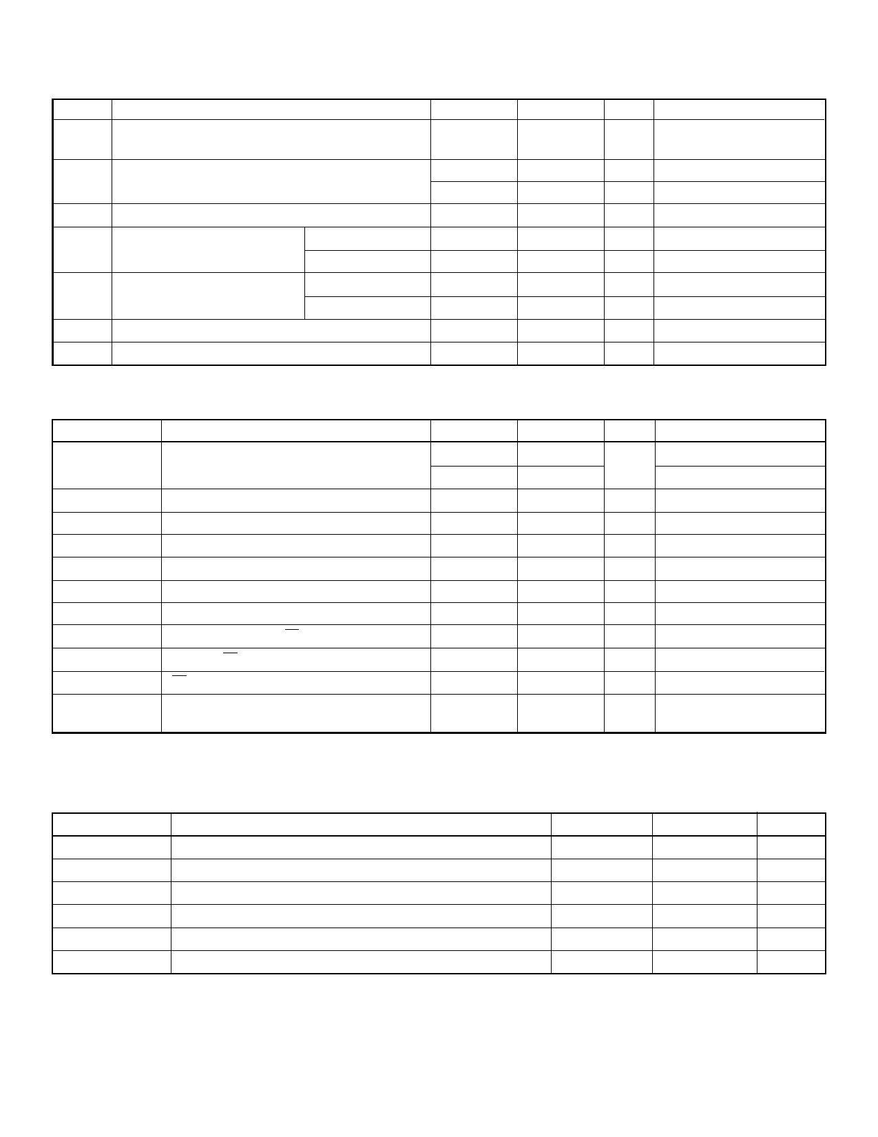
Electrical Characteristics (over recommended commercial operating conditions unless noted)
DC Characteristics
Symbol
Parameter
IDD VDD supply current
IPP Quiescent VPP supply current
Min
Max Units
Conditions
30
mA VDD = VDD max
fCLK = 25MHz
100
µA Outputs high
100
µA Outputs low
IDDQ Quiescent VDD supply current
VOH High-level output
VOL Low-level output
IIH High-level logic input current
IIL
Low-level logic input current
HVOUT
Data out
HVOUT
Data out
VPP - 9V
VDD - 0.5
100
3.75
0.5
1.0
-1.0
µA All VIN = VDD
V
IO= -30mA, VPP = 80V
V IO= -100µA
V
IO = 15mA, VDD = 5V
V IO= 100µA
µA VIH = VDD
µA VIL = 0V
AC Characteristics (TA = 85°C max. Logic signal inputs and Data inputs have tr, tf ≤ 5ns [10% and 90% points])
Symbol
Parameter
Min
Max
Units
Conditions
fCLK
Clock frequency
0.001
0.001
25
VDD = 4.5V, TJ = 25°C
MHz
20
VDD = 4.5V, TJ = 125°C
tWL,tWH
Clock width high or low
20
ns
tSU
Data set-up time before clock rises
0
ns
tH
Data hold time after clock rises
15
ns
tON, tOFF
Time from latch enable to HVOUT
500
ns CL = 15pF
tDHL
Delay time clock to data high to low
38
ns CL = 15pF, VDD = 5.0V
tDLH
Delay time clock to data low to high
38
ns CL = 15pF, VDD = 5.0V
tDLE*
Delay time clock to LE low to high
25
ns
tWLE
Width of LE pulse
25
ns
tSLE
LE set-up time before clock rises
0
ns
tr, tf
Output rise/fall time
1.0
µs CL = 600pF,
HVOUT from 0 to 60V
* tDLE is not required but is recommended to produce stable HV outputs and thus minimize power dissipation and current spikes (allows internal SR output to stabilize).
Recommended Operating Conditions
Symbol
Parameter
VDD
Logic supply voltage
VPP
Output voltage
VIH
High-level input voltage
VIL
Low-level input voltage
fCLK
Clock frequency per register
TA
Operating free-air temperature
Notes: Power-up sequence should be the following:
1. Connect ground.
2. Apply VDD.
3. Set all inputs (Data, CLK, Enable, etc.) to a known state.
4. Apply VPP.
5. The VPP should not drop below VDD or float during operation.
Power-down sequence should be the reverse of the above.
The VPP should not drop below VDD during operation.
2
Min
4.5
12
VDD -0.5V
0
0.001
-40
Max
Units
5.5
V
80
V
V
0.5
V
25
MHz
+85
°C
Share Link: 