WRA-YD-55WW Ver la hoja de datos (PDF) - Microdc power Technology Co., Ltd
Número de pieza
componentes Descripción
Fabricante
WRA-YD-55WW
Microdc power Technology Co., Ltd

WRA-YD-55WW Datasheet PDF : 3 Pages
| |||
WRA-YD-5W&WRB-YD -5W Series
General Specifications
Physical Specifications
Temperature ranges
–Operating
–Case temperature
–40 ℃ ... + 85 ℃
+100 ℃ max.
–Storage
–55 ℃ ... + 125 ℃
Derating
3.5% /K above 70 ℃
Humidity(non condensing)
95 % rel H max.
Reliability, calculated MTBF (MIL-HDBK-217 E)
>1 Mio. h @ + 25 ℃
Isolation voltage
Input/Output
1500 VDC
Isolation capacity
Input/Output
380 pF typ.
Isolation resistance
Input/Output (500 VDC)
> 1000 M Ohm
Switching frequency
Safety standards
300 kHz typ. (Pulse frequency modulation PFM)
UL 60950, IEC 60950, EN 60950
Compliance up to 60 VDC input voltage(SELV limit)
Safety approval
UL /cUL File E188913 (5Vin models pending)
Case material
Baseplate material
Potting material
Weight
Soldering temperature
steel, Nickel plated
non conductive FR4
epoxy (UL 94V-0 rated)
14 g (0.55 oz)
max. 265 °C / 10 sec.
APPLICATION NOTE
Requirement on output load
In order to ensure the product operate efficiently and reliably,in addition to a
max load(namely full load), a minimum load is specified for this kind of
DC/DC converter.Make sure the specified range of input voltage is not
exceeded,the minimum output load no less than 10% load.If the actual
load is less than the specified minimum load, the output ripple may increase
sharply while its efficiency and reliability will reduce greatly.If the actual
output power is very small,please add an appropriate resistor as extra
loading,or contact our company for other lower output power products.
TYPICAL CHARACTERISTICS
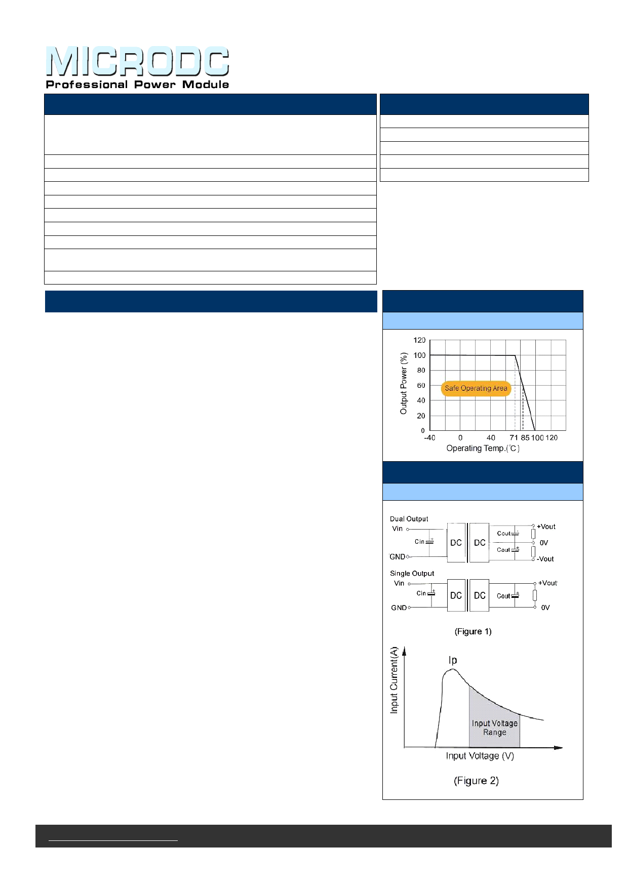
Temperature Derating Graph
Recommended Circuit
All the WRA_YD-5W&WRB_YD-5W Series have been tested according to
the following recommended testing circuit before leaving factory.This series
should be tested under load(See figure 1).
If you want to further decrease the input/output ripple,you can increase
capacitance properly or choose capacitors with low ESR. However, the
capacitance of the output filter capacitor must be proper. If the capacitance
is too big, a startup problem might arise. For every channel of output,
provided the safe and reliable operation is ensured, the greatest capacitance
of its filter capacitor sees (Table 1).
General:
Cin: 5V&12V 100μF
24V&48V 100μF-47μF
Cout: 10μF/100mA
Input current
RECOMMENDED CIRCUIT
Output Graph
While using unstable power source,please ensure the output voltage and
ripple voltage do not exceed indexes of the converter. Input current of
power supply should afford the startup current of this kind of DC/DC module
(See figure 2).
General:Ip≤1.4*Iin-max
No parallel connection or plug and play
http://www.microdc.cn Technical Enquiries-Email:tech@microdc.cn Tel:0086-20-86000646 Page 2 of 3
Share Link: