UPC2711T Ver la hoja de datos (PDF) - Renesas Electronics
Número de pieza
componentes Descripción
Fabricante
UPC2711T Datasheet PDF : 18 Pages
| |||
µPC3215TB
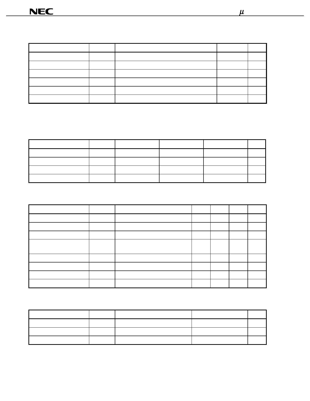
ABSOLUTE MAXIMUM RATINGS
Parameter
Supply Voltage
Circuit Current
Input Power
Power Dissipation
Operating Ambient Temperature
Storage Temperature
Symbol
VCC
ICC
Pin
PD
TA
Tstg
TA = +25°C
TA = +25°C
TA = +25°C
TA = +85°CNote
Conditions
Ratings
6.0
30
+10
270
–40 to +85
–55 to +150
Unit
V
mA
dBm
mW
°C
°C
Note Mounted on 50 × 50 × 1.6-mm epoxy glass PWB, with copper patterning on both sides.
RECOMMENDED OPERATING CONDITIONS
Parameter
Supply Voltage
Operating Ambient Temperature
Input Power
Input Frequency
Symbol
VCC
TA
Pin
fin
MIN.
4.5
–40
–
0.1
TYP.
5.0
+25
–
–
MAX.
5.5
+85
0
2.9
Unit
V
°C
dBm
GHz
ELECTRICAL CHARACTERISTICS (TA = +25°C, VCC = 5.0 V, ZS = ZL = 50 Ω)
Parameter
Circuit Current
Power Gain
Noise Figure
Upper Limit Operating
Frequency
Isolation
Input Return Loss
Output Return Loss
1 dB Compression Point
Symbol
ICC
GP
NF
fu
ISL
RLin
RLout
P-1
Test Conditions
No input signals
f = 1.5 GHz, Pin = –30 dBm
f = 1.5 GHz
3 dB down below from gain at
f = 0.1 GHz
f = 1.5 GHz, Pin = –30 dBm
f = 1.5 GHz, Pin = –30 dBm
f = 1.5 GHz, Pin = –30 dBm
MIN. TYP. MAX. Unit
10.5
14.0
17.5
mA
18.5
20.5
–
dB
–
2.3
3.0
dB
2.5
2.9
–
GHz
39
44
–
dB
10
15
–
dB
6.5
9.5
–
dB
–4
–1.5
–
dBm
STANDARD CHARACTERISTICS (TA = +25°C, VCC = 5.0 V, ZS = ZL = 50 Ω)
Parameter
Saturated Output Power
Output Intercept Point
Gain Flatness
Symbol
PO(sat)
OIP3
∆GP
Test Conditions
Pin = 0 dBm
f1 = 1.5 GHz, f2 = 1.501 GHz
f = 0.1 to 2.15 GHz
Reference Values
+3.5
+10
1.0
Unit
dBm
dBm
dB
4
Data Sheet P14765EJ2V0DS00
Share Link: 