UPC2711T Ver la hoja de datos (PDF) - Renesas Electronics
Número de pieza
componentes Descripción
Fabricante
UPC2711T Datasheet PDF : 18 Pages
| |||
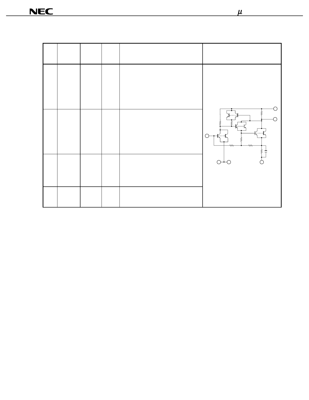
µPC3215TB
PIN EXPLANATION
Applied Pin
Pin
Pin Name Voltage Voltage
No.
(V)
(V)Note
Function and Applications
1 INPUT
0.82 Signal input pin. A internal matching circuit,
configured with resistors, enables 50 Ω
connection over a wideband. A multi-
feedback circuit is designed to cancel the
deviations of hFE and resistance. This pin
must be coupled to signal source with
capacitor for DC cut.
2 GND
3
5
0
Ground pin. This pin should be connected
to system ground with minimum inductance.
Ground pattern on the board should be
formed as wide as possible. All the ground IN
pins must be connected together with wide 1
ground pattern to decrease impedance
difference.
4 OUTPUT
3.8 Signal output pin. A internal matching
circuit, configured with resistors, enables 50
Ω connection over a wideband. This pin
must be coupled to next stage with
capacitor for DC cut.
6
VCC
4.5 to 5.5
Power supply pin. This pin should be
externally equipped with bypass capacitor to
minimize ground impedance.
Internal Equivalent Circuit
VCC
6
4
OUT
25
GND
3
GND
Note Pin voltage is measured at VCC = 5.0 V
Data Sheet P14765EJ2V0DS00
3
Share Link: 