TOP232G Ver la hoja de datos (PDF) - Power Analog Micoelectronics
Número de pieza
componentes Descripción
Fabricante
TOP232G Datasheet PDF : 36 Pages
| |||
TOP232-234
TOPSwitch-FX Family Functional Description
Like TOPSwitch, TOPSwitch-FX is an integrated switched
mode power supply chip that converts a current at the control
input to a duty cycle at the open drain output of a high voltage
power MOSFET. During normal operation the duty cycle of the
power MOSFET decreases linearly with increasing CONTROL
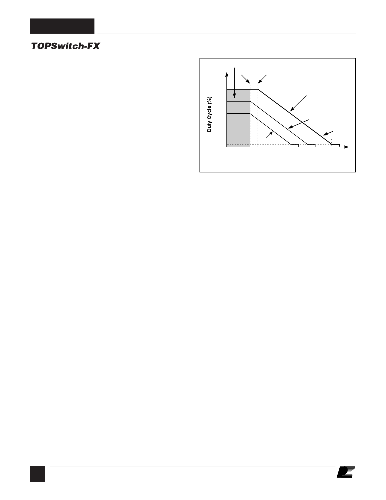
pin current as shown in Figure 4.
Auto-restart
ICD1
IB
78
Slope = PWM Gain
In addition to the three terminal TOPSwitch features, such as the
high voltage start-up, the cycle-by-cycle current limiting, loop
compensation circuitry, auto-restart, thermal shutdown, etc.,
the TOPSwitch-FX incorporates many additional functions that
reduce system cost, increase power supply performance and
design flexibility. A patented high voltage CMOS technology
allows both the high voltage power MOSFET and all the low
voltage control circuitry to be cost effectively integrated onto a
single monolithic chip.
Two terminals, FREQUENCY (available only in Y package)
and MULTI-FUNCTION, have been added to implement some
of the new functions. These terminals can be connected to the
SOURCE pin to operate the TOPSwitch-FX in a TOPSwitch-
like three terminal mode. However, even in this three terminal
mode, the TOPSwitch-FX offers many new transparent features
that do not require any external components:
1. A fully integrated 10 ms soft-start reduces peak currents and
voltages during start-up and practically eliminates output
overshoot in most applications.
2. DCMAX of 78% allows smaller input storage capacitor, lower
input voltage requirement and/or higher power capability.
3. Cycle skipping at minimum pulse width achieves regulation
and very low power consumption at no load.
4. Higher switching frequency of 132 kHz reduces the
transformer size with no noticeable impact on EMI or on
high line efficiency.
5. Frequency jittering reduces EMI.
6. Hysteretic over-temperature shutdown ensures automatic
recovery from thermal fault. Large hysteresis prevents circuit
board overheating.
7. Packages with omitted pins and lead forming provide large
DRAIN creepage distance.
8. Tighter absolute tolerances and smaller temperature vari-
ations on switching frequency, current limit and PWM gain.
The MULTI-FUNCTION pin is usually used for line sensing by
connecting a resistor from this pin to the rectified DC high
voltage bus to implement line over-voltage (OV)/under-voltage
(UV) and line feed forward with DCMAX reduction. In this
mode, the value of the resistor determines the OV/UV thresholds
and the DCMAX is reduced linearly starting from a line voltage
above the under-voltage threshold. In high efficiency
applications, this pin can be used in the external current limit
mode instead, to reduce the current limit externally (to a value
47
IM = 140 µA
IM < IM(DC)
1.5
IM = 190 µA
1.5 1.9
5.5 5.9
IC (mA)
PI-2504-072799
Figure 4. Relationship of Duty Cycle to CONTROL Pin Current.
close to the operating peak current), by connecting the pin to
SOURCE through a resistor. The same pin can also be used as
a remote ON/OFF and a synchronization input in both modes.
The FREQUENCY pin in the TO-220 package sets the switching
frequency to the default value of 132 kHz when connected to
SOURCE pin. A half frequency option can be chosen by
connecting this pin to CONTROL pin instead. Leaving this pin
open is not recommended.
CONTROL (C) Pin Operation
The CONTROL pin is a low impedance node that is capable of
receiving a combined supply and feedback current. During
normal operation, a shunt regulator is used to separate the
feedback signal from the supply current. CONTROL pin voltage
V is the supply voltage for the control circuitry including the
C
MOSFET gate driver. An external bypass capacitor closely
connected between the CONTROL and SOURCE pins is
required to supply the instantaneous gate drive current. The
total amount of capacitance connected to this pin also sets the
auto-restart timing as well as control loop compensation.
When rectified DC high voltage is applied to the DRAIN pin
during start-up, the MOSFET is initially off, and the CONTROL
pin capacitor is charged through a switched high voltage current
source connected internally between the DRAIN and CONTROL
pins. When the CONTROL pin voltage VC reaches
approximately 5.8 V, the control circuitry is activated and the
soft-start begins. The soft-start circuit gradually increases the
duty cycle of the MOSFET from zero to the maximum value
over approximately 10 ms. If no external feedback/supply
current is fed into the CONTROL pin by the end of the soft-start,
the high voltage current source is turned off and the CONTROL
pin will start discharging in response to the supply current
drawn by the control circuitry. If the power supply is designed
properly, and no fault condition such as open loop or shorted
output exists, the feedback loop will close, providing external
4B
7/01
Share Link: 