TC911B Ver la hoja de datos (PDF) - TelCom Semiconductor Inc => Microchip
Número de pieza
componentes Descripción
Fabricante
TC911B Datasheet PDF : 5 Pages
| |||
AUTO-ZEROED MONOLITHIC
OPERATIONAL AMPLIFIERS
TC911A
TC911B
ABSOLUTE MAXIMUM RATINGS*
Total Supply Voltage (VDD to VSS) ........................... +18V
Input Voltage ........................ (VDD + 0.3V) to (VSS – 0.3V)
Current into Any Pin .................................................10mA
While Operating ................................................100µA
Storage Temperature Range ................ – 65°C to +150°C
Lead Temperature (Soldering, 10 sec) ................. +300°C
Operating Temperature Range
C Device ................................................ 0°C to +70°C
Package Power Dissipation (TA = ≤ 70°C)
Plastic DIP ...................................................... 730mW
Plastic SOIC ................................................... 470mW
*Static-sensitive device. Unused devices should be stored in conductive
material. Stresses above those listed under “Absolute Maximum Ratings”
may cause permanent damage to the device. These are stress ratings only
and functional operation of the device at these or any other conditions
above those indicated in the operational sections of the specifications is not
implied.
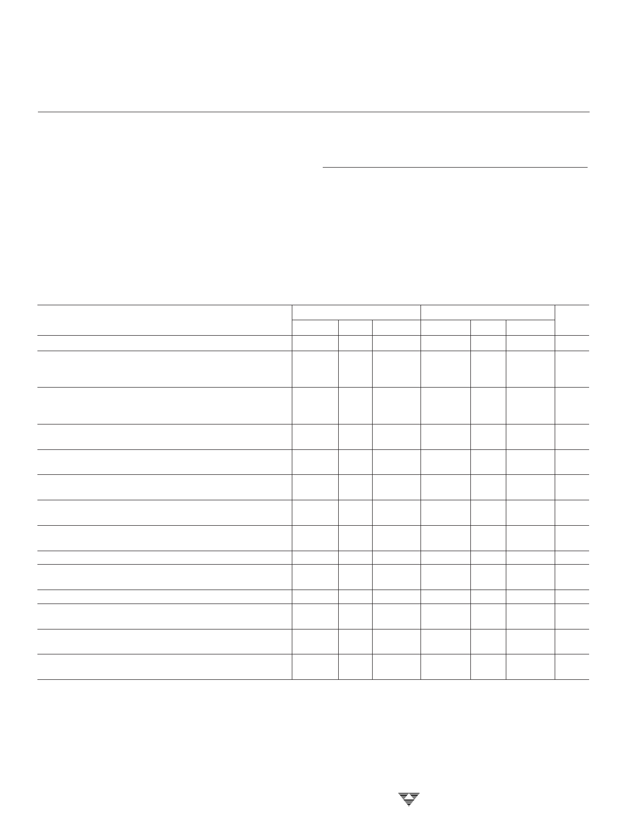
ELECTRICAL CHARACTERISTICS: VS = ±5V, TA = +25°C, unless otherwise indicated.
Symbol Parameter
VOS
TCVOS
IB
Input Offset Voltage
Average Temperature
Coefficient of Input
Offset Voltage
Average Input Bias
Current
IOS
Average Input
Offset Current
eN
Input Voltage Noise
CMRR
CMVR
AOL
VOUT
BW
SR
PSRR
VS
IS
Common-Mode
Rejection Ratio
Common-Mode
Voltage Range
Open-Loop Voltage
Gain
Output Voltage Swing
Closed Loop
Bandwidth
Slew Rate
Power Supply
Rejection Ratio
Operating Supply
Voltage Range
Quiescent Supply
Current
Test Conditions
TA = +25°C
0°C ≤ TA ≤ +70°C
–25°C ≤ TA ≤ +85°C
(Note 1)
TA = +25°C
0°C ≤ TA ≤ +70°C
–25°C ≤ TA ≤ +85°C
TA = +25°C
TA = +85°C
0.1 to 1 Hz, RS ≤ 100Ω
0.1 to 10 Hz, RS ≤ 100Ω
VSS ≤ VCM ≤ VDD – 2.2
TC911A
Min Typ Max
—
5
15
—
0.05 0.15
—
0.05 0.15
—
—
70
—
—
3
—
—
4
—
5
20
—
—
1
—
0.65
—
—
11
—
110
116
—
TC911B
Min Typ Max
—
15
30
—
0.1
0.25
—
0.1
0.25
—
—
120
—
—
4
—
—
6
—
10
40
—
—
1
—
0.65
—
—
11
—
105
110
—
VSS
— VDD – 2
VSS
RL = 10 kΩ, VOUT = ±4V 115
120
—
110
— VDD – 2
120
—
RL = 10 kΩ
VSS + 0.3 — VDD – 0.9 VSS + 0.3
Closed Loop Gain = +1 —
1.5
—
—
— VDD – 0.9
1.5
—
RL = 10 kΩ, CL = 50 pF
—
2.5
—
±3.3V to ±5.5V
112
—
—
—
2.5
—
105
—
—
Split Supply
Single Supply
VS = ±5V
±3.3
—
±8
6.5
—
16
—
350
600
±3.3
—
±8
6.5
—
16
—
—
800
NOTES: 1. Characterized; not 100% tested.
Unit
µV
µV/°C
µV/°C
pA
nA
nA
pA
nA
µVP-P
µVP-P
dB
V
dB
V
MHz
V/µs
dB
V
V
µA
3-264
TELCOM SEMICONDUCTOR, INC.
Share Link: 