LT1160 Ver la hoja de datos (PDF) - Linear Technology
Número de pieza
componentes Descripción
Fabricante
LT1160 Datasheet PDF : 16 Pages
| |||
LT1160/LT1162
APPLICATIONS INFORMATION
Power MOSFET Selection
Since the LT1160 (or 1/2 LT1162) inherently protects the
top and bottom MOSFETs from simultaneous conduction,
there are no size or matching constraints. Therefore selec-
tion can be made based on the operating voltage and
RDS(ON) requirements. The MOSFET BVDSS should be
greater than the HV and should be increased to approxi-
mately (2)(HV) in harsh environments with frequent fault
conditions. For the LT1160 maximum operating HV supply
of 60V, the MOSFET BVDSS should be from 60V to 100V.
The MOSFET RDS(ON) is specified at TJ = 25°C and is
generally chosen based on the operating efficiency re-
quired as long as the maximum MOSFET junction tem-
perature is not exceeded. The dissipation while each
MOSFET is on is given by:
P = D(IDS)2(1+∂)RDS(ON)
Where D is the duty cycle and ∂ is the increase in RDS(ON)
at the anticipated MOSFET junction temperature. From this
equation the required RDS(ON) can be derived:
( ) ( ) RDS(ON) =
P
2
D IDS 1+ ∂
For example, if the MOSFET loss is to be limited to 2W
when operating at 5A and a 90% duty cycle, the required
RDS(ON) would be 0.089Ω/(1 + ∂). (1 + ∂) is given for each
MOSFET in the form of a normalized RDS(ON) vs tempera-
ture curve, but ∂ = 0.007/°C can be used as an approxima-
tion for low voltage MOSFETs. Thus, if TA = 85°C and the
available heat sinking has a thermal resistance of 20°C/W,
the MOSFET junction temperature will be 125°C and
∂ = 0.007(125 – 25) = 0.7. This means that the required
RDS(ON) of the MOSFET will be 0.089Ω/1.7 = 0.0523Ω,
which can be satisfied by an IRFZ34 manufactured by
International Rectifier.
Transition losses result from the power dissipated in each
MOSFET during the time it is transitioning from off to on,
or from on to off. These losses are proportional to (f)(HV)2
and vary from insignificant to being a limiting factor on
operating frequency in some high voltage applications.
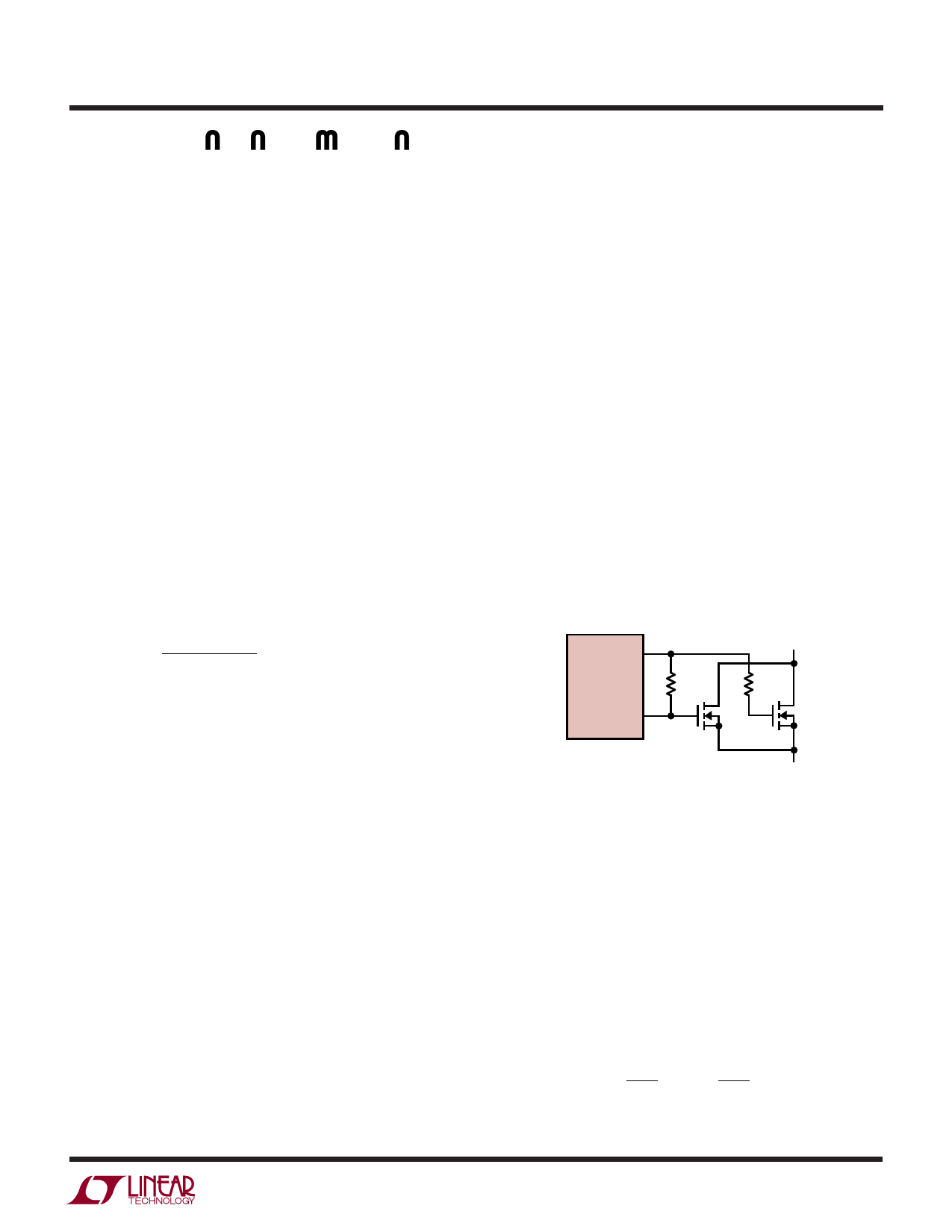
Paralleling MOSFETs
When the above calculations result in a lower RDS(ON) than
is economically feasible with a single MOSFET, two or
more MOSFETs can be paralleled. The MOSFETs will
inherently share the currents according to their RDS(ON)
ratio as long as they are thermally connected (e.g., on a
common heat sink). The LT1160 top and bottom drivers
can each drive five power MOSFETs in parallel with only a
small loss in switching speeds (see Typical Performance
Characteristics). A low value resistor (10Ω to 47Ω) in
series with each individual MOSFET gate may be required
to “decouple” each MOSFET from its neighbors to prevent
high frequency oscillations (consult manufacturer’s rec-
ommendations). If gate decoupling resistors are used the
corresponding gate feedback pin can be connected to any
one of the gates as shown in Figure 1.
Driving multiple MOSFETs in parallel may restrict the
operating frequency to prevent overdissipation in the
LT1160 (see the following Gate Charge and Driver Dissi-
pation).
GATE DR
LT1160
RG*
RG*
GATE FB
*OPTIONAL 10Ω
1160 F01
Figure 1. Paralleling MOSFETs
Gate Charge and Driver Dissipation
A useful indicator of the load presented to the driver by a
power MOSFET is the total gate charge QG, which includes
the additional charge required by the gate-to-drain swing.
QG is usually specified for VGS = 10V and VDS = 0.8VDS(MAX).
When the supply current is measured in a switching
application, it will be larger than given by the DC electrical
characteristics because of the additional supply current
associated with sourcing the MOSFET gate charge:
ISUPPLY
=
IDC
+
⎛
⎝⎜
dQG
dt
⎞
⎠⎟
TOP
+
⎛
⎝⎜
dQG
dt
⎞
⎠⎟
BOTTOM
11602fb
9
Share Link: 