T5760 Ver la hoja de datos (PDF) - Atmel Corporation
Número de pieza
componentes Descripción
Fabricante
T5760 Datasheet PDF : 32 Pages
| |||
T5760 / T5761
The value of CL should be optimized for the individual
board layout to achieve the exact value of fXTO (the best
way is to use a crystal with known load resonance fre-
quency to find the right value for this capacitor) and
hereby of fLO. When designing the system in terms of re-
ceiving bandwidth and local oscillator accuracy, the
accuracy of the crystal and the XTO must be considered.
If a crystal with $30 ppm adjustment tolerance at 25_C
, $50ppm over Temperature –40_C to 105_C, $10 ppm
of total aging and a CM ( motional capacitance ) of 7 fF
is used, an additional XTO pulling of $30 ppm has to be
added.
The resulting total LO tolerance of $120ppm agrees with
the receiving bandwidth specification of the
T5760/T5761 if the T5750 has also a total LO tolerance
of $120 ppm.
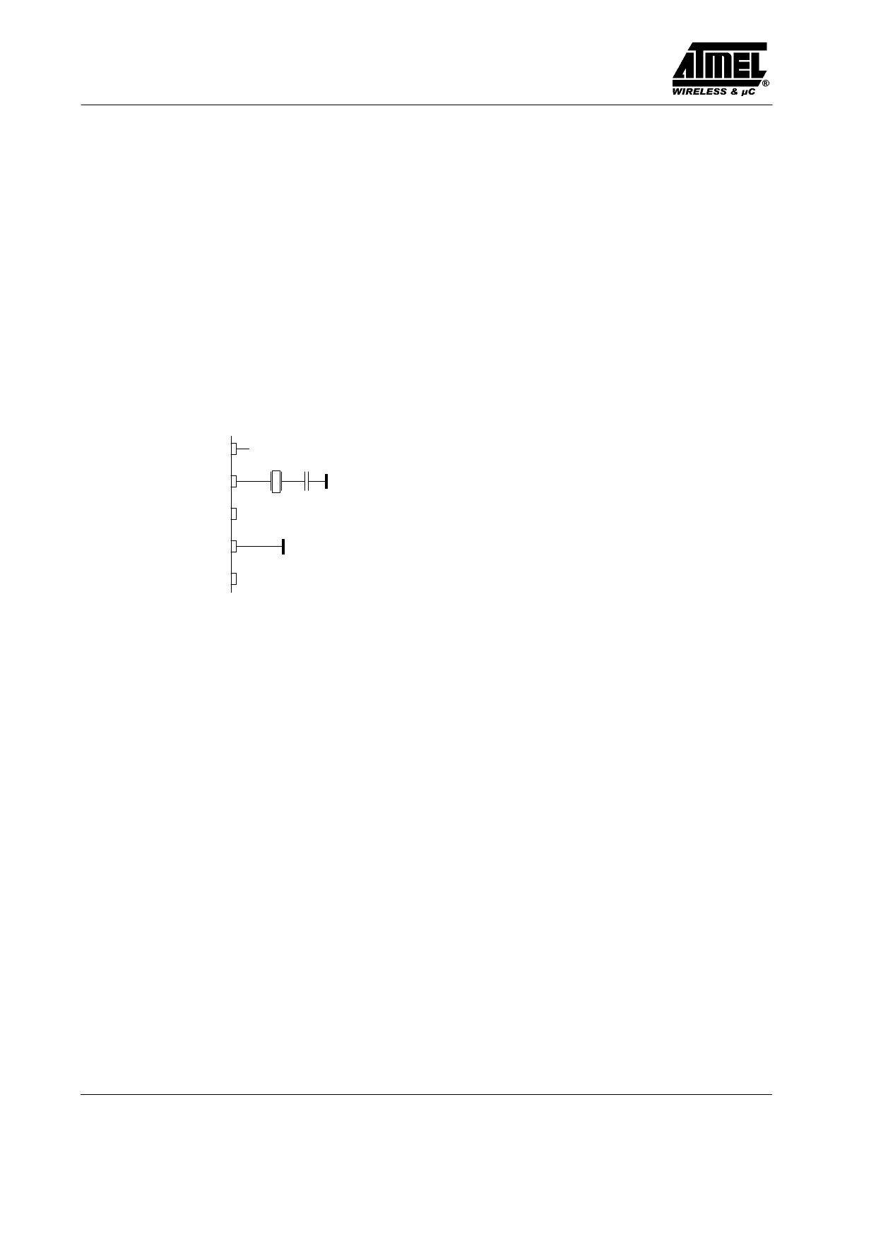
VS
DVCC
CL
XTAL
n.c.
TEST 3
TEST 2
Figure 4. XTO peripherals
The nominal frequency fLO is determined by the RF input
frequency fRF and the IF frequency fIF using the following
formula (low side injection):
fLO = fRF – fIF
To determine fLO , the construction of the IF filter must
be considered at this point. The nominal IF frequency is
fIF = 950 kHz. To achieve a good accuracy of the filter
corner frequencies, the filter is tuned by the crystal fre-
quency fXTO. This means that there is a fixed relation
between fIF and fLO.
fIF = fLO / 915
The relation is designed to achieve the nominal IF fre-
quency of fIF = 950 kHz for the 868.3 MHz version. For
the 915 MHz version an IF frequency of fIF = 1.0 MHz
results.
The RF input either from an antenna or from a RF genera-
tor must be transformed to the RF input Pin LNA_IN. The
input impedance of that pin is provided in the electrical
parameters. The parasitic board inductances and capaci-
tances influence the input matching. The RF receiver
T5760/T5761 exhibits its highest sensitivity if the LNA
is power matched. This makes the matching to an SAW
filter as well as to 50 W or an antenna more easy.
Figure 33 shows a typical input matching network for fRF
= 868.3 MHz to 50 W. Figure 34 illustrates an according
input matching for 868.3 MHz to an SAW. The input
matching network shown in Figure 33 is the reference net-
work for the parameters given in the electrical
characteristics.
Analog Signal Processing
IF Filter
The signals coming from the RF front end are filtered by
the fully integrated 4th-order IF filter. The IF center fre-
quency is fIF = 950 kHz for applications where fRF =
868.3 MHz and fIF =1.0 MHz for fRF = 915 MHz. The
nominal bandwidth is 600 kHz.
Limiting RSSI Amplifier
The subsequent RSSI amplifier enhances the output
signal of the IF amplifier before it is fed into the demod-
ulator. The dynamic range of this amplifier is
DRRSSI = 60 dB. If the RSSI amplifier is operated within
its linear range, the best S/N ratio is maintained in ASK
mode. If the dynamic range is exceeded by the transmitter
signal, the S/N ratio is defined by the ratio of the maxi-
mum RSSI output voltage and the RSSI output voltage
due to a disturber. The dynamic range of the RSSI ampli-
fier is exceeded if the RF input signal is about 60 dB
higher compared to the RF input signal at full sensitivity.
In FSK mode the S/N ratio is not affected by the dynamic
range of the RSSI amplifier, because only the hard limited
signal from a high gain limiting amplifier is used by the
demodulator.
The output voltage of the RSSI amplifier is internally
compared to a threshold voltage VTh_red. VTh_red is deter-
mined by the value of the external resistor RSens. RSens is
connected between Pin SENS and GND or VS. The output
of the comparator is fed into the digital control logic. By
this means it is possible to operate the receiver at a lower
sensitivity.
If RSens is connected to GND, the receiver switches to full
sensitivity. It is also possible to connect the Pin SENS di-
rectly to GND to get the maximum sensitivity.
If RSens is connected to VS, the receiver operates at a
lower sensitivity. The reduced sensitivity is defined by the
value of RSens, the maximum sensitivity by the signal-to-
noise ratio of the LNA input. The reduced sensitivity
depends on the signal strength at the output of the RSSI
amplifier.
Since different RF input networks may exhibit slightly
different values for the LNA gain, the sensitivity values
given in the electrical characteristics refer to a specific
input matching. This matching is illustrated in figure 33
4 (32)
Rev. A2, 19-Oct-00
Preliminary Information
Share Link: 