T35L6464A Ver la hoja de datos (PDF) - Taiwan Memory Technology
Número de pieza
componentes Descripción
Fabricante
T35L6464A Datasheet PDF : 16 Pages
| |||
tm TE
CH
T35L6464A
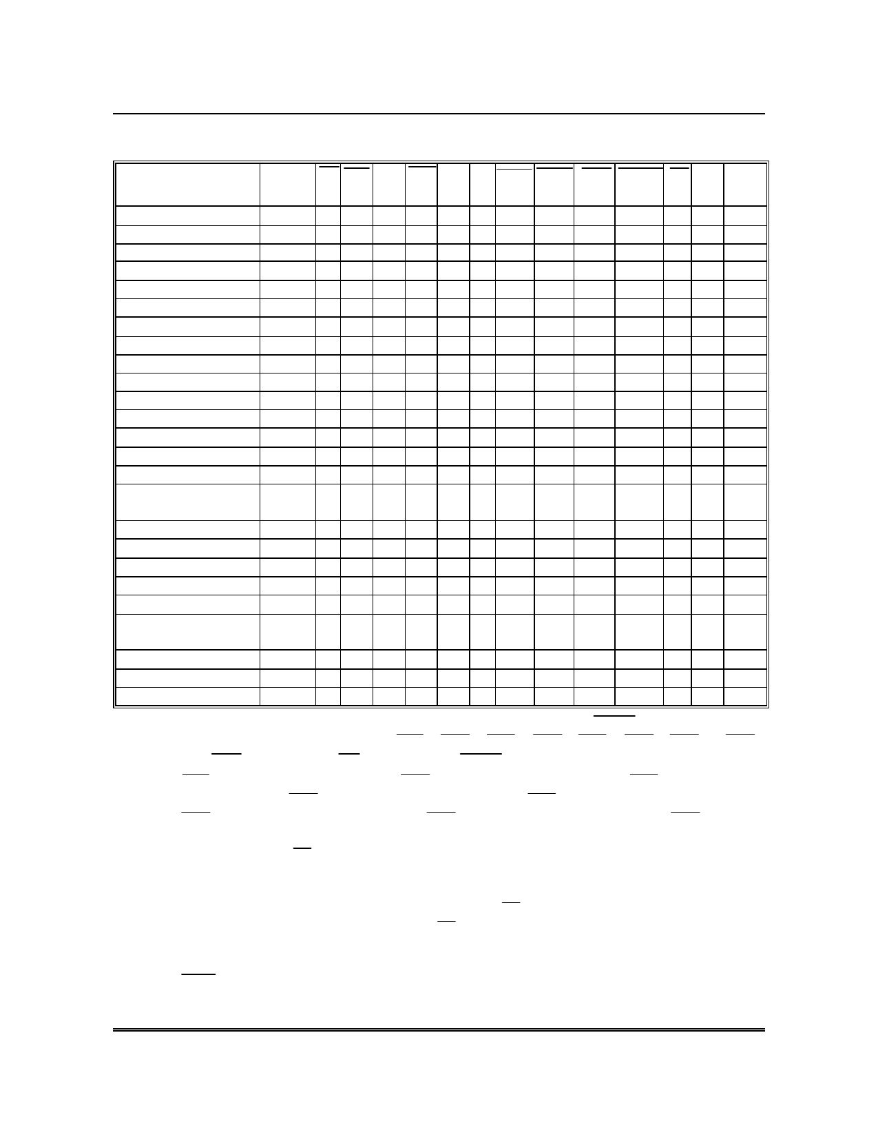
TRUTH TABLE
OPERATION ADDRESS CE CE2 CE2 CE3 CE3 ZZ ADSP ADSC ADV WRITE OE CLK DQ
USED
Deselected Cycle, Power Down
Deselected Cycle, Power Down
Deselected Cycle, Power Down
Deselected Cycle, Power Down
None H X X X X L X
L
X
None L X X X L L L
X
X
None L X L X X L L
X
X
None L X X H X L L
X
X
X
X L-H High-Z
X
X L-H High-Z
X
X L-H High-Z
X
X L-H High-Z
Deselected Cycle, Power Down
None L H X X X L L
X
X
Deselected Cycle, Power Down
None L X X X L L H
L
X
Deselected Cycle, Power Down
None L X L X X L H
L
X
X
X L-H High-Z
X
X L-H High-Z
X
X L-H High-Z
Deselected Cycle, Power Down
Deselected Cycle, Power Down
Snooze Cycle, Power Down
None L X X H X L H
L
X
None L H X X X L H
L
X
None X X X X X H X
X
X
X
X L-H High-Z
X
X L-H High-Z
X
X X High-Z
READ Cycle, Begin Burst
READ Cycle, Begin Burst
WRITE Cycle, Begin Burst
External L L H L H L L
X
X
External L L H L H L L
X
X
External L L H L H L H
L
X
X
L L-H Q
X
H L-H High-Z
L
X L-H D
READ Cycle, Begin Burst
External L L H L H L H
L
X
READ Cycle, Begin Burst
External L L H L H L H
L
X
READ Cycle, Continue Burst
Next X X X X X L H
H
L
H
L L-H Q
H
H L-H High-Z
H
L L-H Q
READ Cycle, Continue Burst
READ Cycle, Continue Burst
READ Cycle, Continue Burst
Next X X X X X L H
H
L
Next H X X X X L X
H
L
Next H X X X X L X
H
L
H
H L-H High-Z
H
L L-H Q
H
H L-H High-Z
WRITE Cycle, Continue Burst
Next X X X X X L H
H
L
WRITE Cycle, Continue Burst
Next H X X X X L X
H
L
READ Cycle, Suspend Burst
Current X X X X X L H
H
H
READ Cycle, Suspend Burst
Current X X X X X L H
H
H
READ Cycle, Suspend Burst
Current H X X X X L X
H
H
READ Cycle, Suspend Burst
Current H X X X X L X
H
H
L
X L-H D
L
X L-H D
H
L L-H Q
H
H L-H High-Z
H
L L-H Q
H
H L-H High-Z
WRITE Cycle, Suspend Burst
Current X X X X X L H
H
H
WRITE Cycle, Suspend Burst
Current H X X X X L X
H
H
L
X L-H D
L
X L-H D
Note: 1. X means "don't care." H means logic HIGH. L means logic LOW. WRITE = L means any one
or more byte write enable signals ( BW1, BW2 , BW3 , BW4 , BW5 , BW6 , BW7 or BW8 )
and BWE are LOW, or GW equals LOW. WRITE = H means all byte write signal are HIGH.
2. BW1= enables write to DQ1-DQ8. BW2 = enables write to DQ9-DQ16. BW3 = enables write
to DQ17-DQ24. BW4 =enables write to DQ25-DQ32. BW5 = enables write to DQ33-DQ40.
BW6 = enables write to DQ41-DQ48. BW7 = enables write to DQ49-DQ56. BW8 = enables
write to DQ57-DQ64.
3. All inputs except OE must meet setup and hold times around the rising edge ( LOW to HIGH)
of CLK.
4. Suspending burst generates wait cycle.
5. For a write operation following a read operation. OE must be HIGH before the input data
required setup time plus High-Z time for OE and staying HIGH throughout the input data hold
time.
6. This device contains circuitry that will ensure the outputs will be High-Z during power-up.
7. ADSP = LOW along with chip being selected always initiates an internal READ cycle at the L-H
edge of CLK. A WRITE cycle can be performed by setting WRITE LOW for the CLK L-H edge
of the subsequent wait cycle. Refer to WRITE timing diagram for clarification.
Taiwan Memory Technology, Inc. reserves the right P. 6
to change products or specifications without notice.
Publication Date: AUG. 1998
Revision: E
Share Link: 