T35L6432A Ver la hoja de datos (PDF) - Taiwan Memory Technology
Número de pieza
componentes Descripción
Fabricante
T35L6432A Datasheet PDF : 15 Pages
| |||
tm TE
CH
T35L6432A
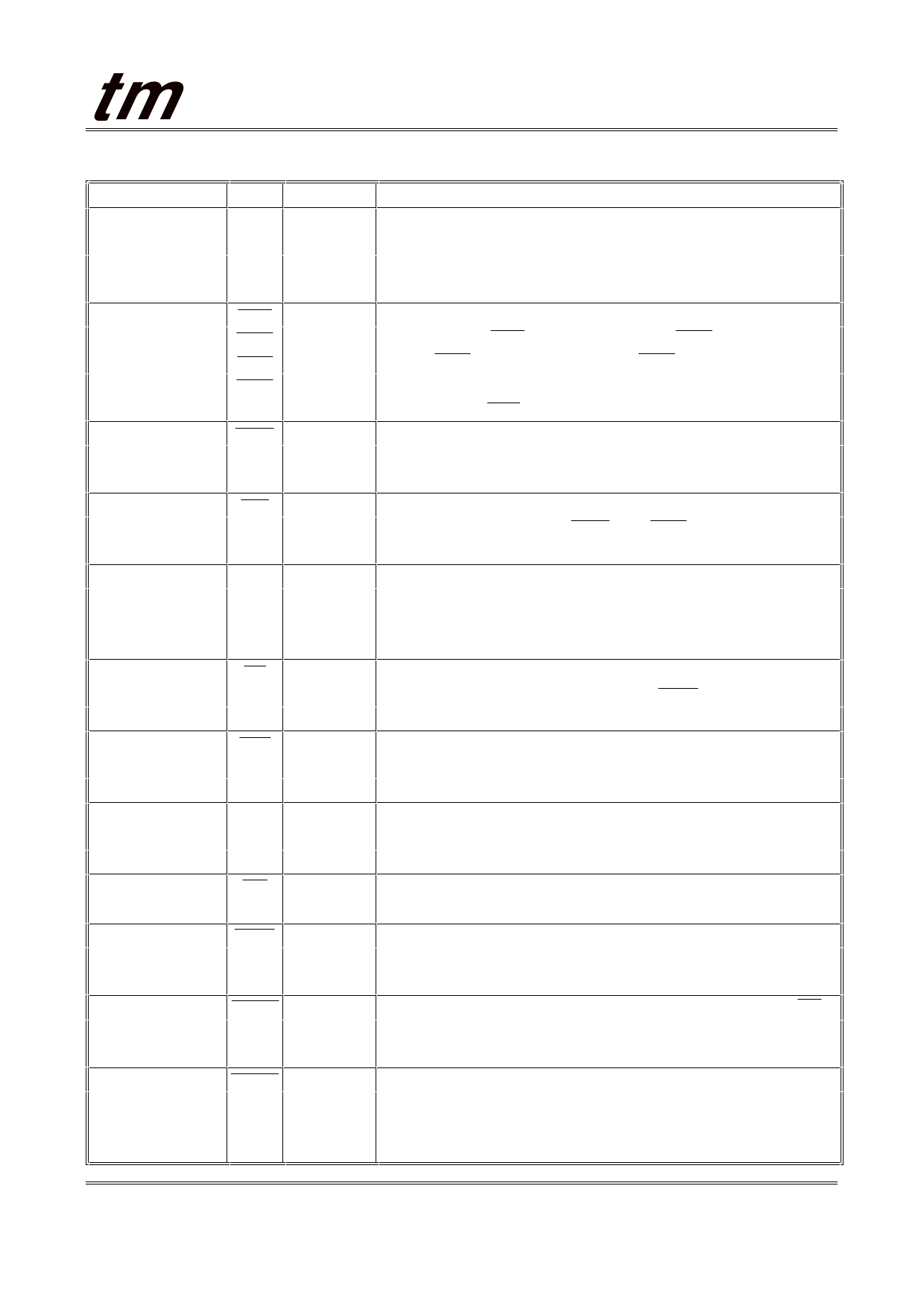
PIN DESCRIPTIONS
QFP PINS
32-37, 44-49,
81, 82, 99, 100,
93-96
87
88
89
98
92
97
86
83
84
85
SYM. TYPE
DESCRIPTION
A0- Input- Addresses: These inputs are registered and must meet the setup and
A15 Synchronous hold times around the rising edge of CLK. The burst counter -
generates internal addresses associated with A0 and A1,during
burst cycle and wait cycle.
BW1 Input- Byte Write: A byte write is LOW for a WRITE cyle and HIGH for
BW2 Synchronous a READ cycle. BW1 controls DQ1-DQ8. BW2 controls DQ9-
BW3
DQ16. BW3 controls DQ17-DQ24. BW4 controls DQ25-DQ32.
BW4
Data I/O are high impedance if either of these inputs are LOW ,
conditioned by BWE being LOW.
BWE Input- Write Enable: This active LOW input gates byte write operations
Synchronous and must meet the setup and hold times around the rising edge of
CLK.
GW Input- Global Write: This active LOW input allows a full 32-bit WRITE
Synchronous to occur independent of the BWE and BWn lines and must meet
the setup and hold times around the rising edge of CLK.
CLK Input- Clock: This signal registers the addresses, data, chip enables, write
Synchronous control and burst control inputs on its rising edge. All synchronous
inputs must meet setup and hold times around the clock's rising
edge.
CE Input- Synchronous Chip Enable: This active LOW input is used to enable
Synchronous the device and conditions internal use of ADSP. This input is
sampled only when a new external address is loaded.
CE2 Input- Synchronous Chip Enable: This active LOW input is used to enable
Synchronous the device. This input is sampled only when a new external address
is loaded. This input can be used for memory depth expansion.
CE2 Input- Synchronous Chip Enable: This active HIGH input is used to enable
Synchronous the device. This input is sampled only when a new external address
is loaded. This input can be used for memory depth expansion.
OE
Input Output enable: This active LOW asynchronous input enables the
data output drivers.
ADV Input- Address Advance: This active LOW input is used to control the
Synchronous internal burst counter. A HIGH on this pin generates wait cycle
(no address advance).
ADSP Input- Address Status Processor: This active LOW input, along withCE
Synchronous being LOW, causes a new external address to be registered and a
READ cycle is initiated using the new address.
ADSC Input- Address Status Controller:This active LOW input causes device to
Synchronous be deselected or selected along with new external address to be
registered. A READ or WRITE cycle is initiated depending upon
write control inputs.
Taiwan Memory Technology, Inc. reserves the right P. 3
to change products or specifications without notice.
Publication Date: DEC. 1998
Revision:A
Share Link: 