T35L6432A Ver la hoja de datos (PDF) - Taiwan Memory Technology
Número de pieza
componentes Descripción
Fabricante
T35L6432A Datasheet PDF : 15 Pages
| |||
tm TE
CH
GENERAL DESCRIPTION (continued)
chip enable (CE), depth- expansion chip enables
(CE2 and CE2),burst control inputs
(ADSC ,ADSP, and ADV ), write enables
(BW1, BW2 , BW3, BW4 , and BWE ), and
global write (GW ).
Asynchronous inputs include the output
enable (OE ),Snooze enable (ZZ) and burst mode
control (MODE). The data outputs (Q), enabled
by OE , are also asynchronous.
Addresses and chip enables are registered
with either address status processor (ADSP) or
address status controller (ADSC ) input pins.
Subsequent burst addresses can be internally
generated as controlled by the burst advance pin
(ADV ).
Address, data inputs, and write controls are
registered on-chip to initiate self-timed WRITE
cycle. WRITE cycles can be one to four bytes
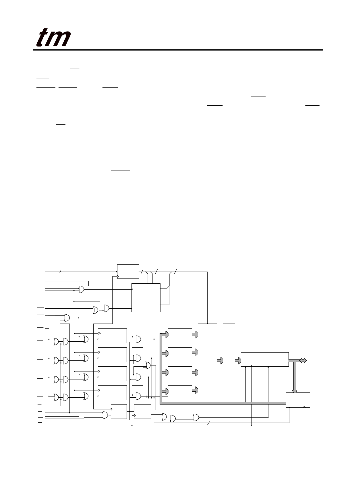
FUNCTIONAL BLOCK DIAGRAM
T35L6432A
wide as controlled by the write control inputs.
Individual byte write allows individual byte to be
written. BW1 controls DQ1-DQ8. BW2
controls DQ9-DQ16. BW3 controls DQ17-DQ
24. BW4 controls DQ25-DQ32. BW1,
BW2 , BW3, and BW4 can be active only with
BWE being LOW. GW being LOW causes all
bytes to be written. WRITE pass-through
capability allows written data available at the
output for the immediately next READ cycle.
This device also incorporates pipelined enable
circuit for easy depth expansion without penalizing
system performance. The T35L6432A operates
from a 3.3V +10%/-5% power supply. The device
is ideally suited for Pentium™, 680X0, and Power
PC™ systems and for systems that are benefited
from a wide synchronous data bus.
16
A0-A15
MODE
ADV
CLK
ADSC
ADSP
ADDRESS
16
14
16
REGISTER
A0 A1
DO D1 Q1
A1'
BINARY
COUNTER
& LOGIC
Q0 A0'
CLR
BWE
BW4
BW3
BW2
BW1
GW
CE
CE2
CE2
OE
BYTE 4
WRITE REGISTER
BYTE 3
WRITE REGISTER
BYTE 2
WRITE REGISTER
BYTE 1
WRITE REGISTER
ENABLE
REGISTER
PIPELINED
ENABLE
8
8
BYTE 4
WRITE DRIVER
8
8
BYTE 3
WRITE DRIVER
32
32
64K x 8 x 4
MEMORY
ARRAY
SENSE
AMPS
OUTPUT
REGISTERS
OUTPUT
BUFFERS
32
DQ1
¡E
¡E
8
8
BYTE 2
¡E
DQ32
WRITE DRIVER
8
8
BYTE 1
WRITE DRIVER
INPUT
REGISTERS
4
Note: 1. The Functional Block Diagram illustrates simplified device operation. See Truth Table, pin
descriptions and timing diagrams for detailed information.
Taiwan Memory Technology, Inc. reserves the right P. 2
to change products or specifications without notice.
Publication Date: DEC. 1998
Revision: A
Share Link: 