ST2L01 Ver la hoja de datos (PDF) - STMicroelectronics
Número de pieza
componentes Descripción
Fabricante
ST2L01 Datasheet PDF : 12 Pages
| |||
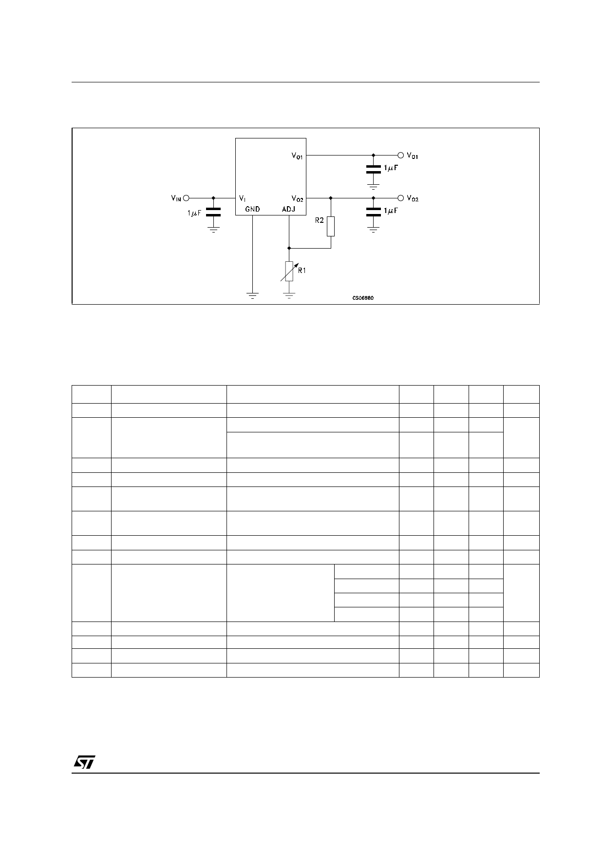
TYPICAL APPLICATION CIRCUIT
ST2L01
VO = VREF (1 + RR12 )+IADJR1
Note:
CO1 value could be lowered down to 470nF Ceramic Capacitor (X7R);
CI, CO1 and CO2 capacitors must be located not more than 0.5" from the outputs pins of the device.
For more details about Capacitors read the "Application Hints"
ELECTRICAL CHARACTERISTICS OF OUTPUT 1 (VI=5V, IO1=10mA Tj = 0 to 125°C unless otherwise
specified. Typical values are referred at Tj = 25°C, CI = 1µF (Tantalum), CO1 = CO1 =1µF (X7R)
Symbol
Parameter
Test Conditions
Min. Typ. Max. Unit
II Input Current
VO1 Output Voltage 1
∆VO1 Line Regulation 1
∆VOUT1 Load Regulation 1
VD1 Dropout Voltage 1
tTR Transient Response
ISC1
IO1
SVR1
Current Limit 1
Minimum Load Current 1
Supply Voltage Rejection
eN1
∆VO1
∆VO1
Thermal Regulation
Output Noise
Temperature Stability
Long Term Stability
IO1 = IO2 =0
Tj = 0 to 125°C
Tj = 25°C
IO1 = 5mA to 1A
Tj = 0 to 125°C
VI = 4.75 to 5.25V
VI = 4.75 to 5.25V
IO = 0.01 to 1A (Note 1)
IO = 1A
(Note 2)
Tj = 0 to 125°C
IO = 10 to 500mA trise = tfall = 1µs
(Note 3, 5)
RL = 0
Tj = 0 to 125°C
Tj = 0 to 125°C (Note 4)
VI = 5 ±0.25V
IO1 = 100 mA
Tj = 0 to 125°C
(Note 5)
fI = 100Hz
fI = 1KHz
fI = 10KHz
fI = 100KHz
IO = 1A,
tPULSE = 30ms (Note 5)
B= 10Hz to 10KHz (Note 5)
Tj = 0 to 125°C (Note 5)
Tj = 125°C, 1000Hrs (Note 5)
15
28
mA
3.23 3.3 3.37
V
3.2 3.3 3.4
0.1
6
mV
3
12
mV
1.1 1.3
V
<1
µs
1
0
60
68
60
70
50
65
30
38
0.1
40
0.5
0.3
A
mA
dB
%/W
µVrms
%VO
%VO
Note 1: Low duty cycle pulse testing with Kelvin connections are required in order to maintain accurate data
Note 2: Dropout Voltage is defined as the minimum differential voltage between VI and VO required to mantain regulation at VO. It is measured
when the output voltage drops 1% below its nominal value.
Note 3: Transient response is defined with a step change in load from 10mA to 500mA as the time from the load step until the output voltage
reaches it’s minimum value.
Note 4: Minimum load current is defined as the minimum current required at the output in order for the output voltage to maintain regulation.
Note 5: Guaranteed by design, not tested in production.
3/12
Share Link: 