SSGSC34119 Ver la hoja de datos (PDF) - Secos Corporation.
Número de pieza
componentes Descripción
Fabricante
SSGSC34119 Datasheet PDF : 9 Pages
| |||
Elektronische Bauelemente
SSGSC34119
Low Power Audio Amplifier
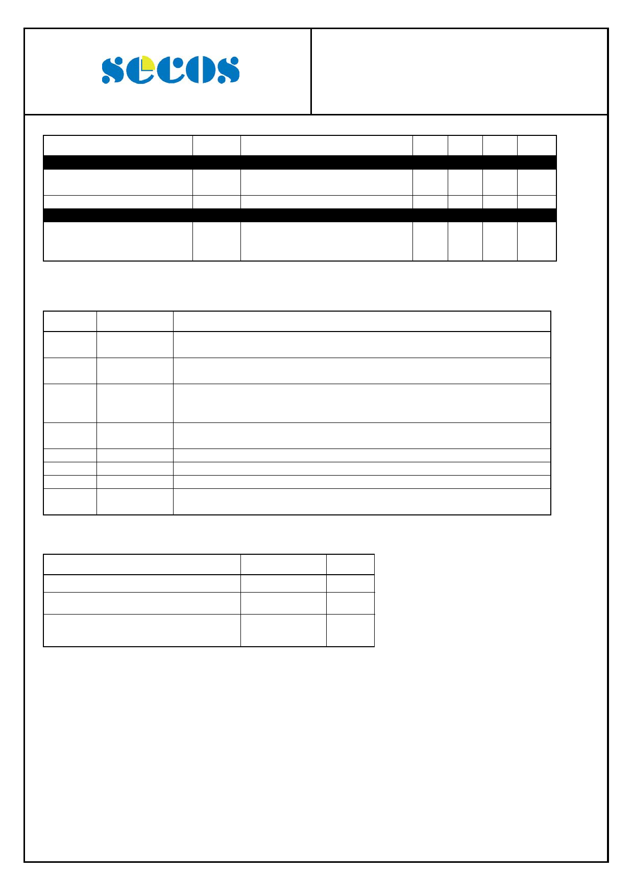
ELECTRICAL CHARACTERISTICS (Cont’d)
Parameter
Symbol
Test Conditions
Chip Disable (Pin1)
Input Voltage
VIL
Low
VIH
High
Input Resistance
RCD
VCC = VCD = 16V
Power Supply
Power Supply Current
ICC3
ICC16
ICCD
VCC = 3V, RL = ∞ , CD = 0.8V
VCC = 16V, RL = ∞ , CD = 0.8V
VCC = 3V, RL = ∞ , CD = 2.0V
Note: Currents into a pin are positive; currents out of a pin are negative.
Min Typ Max Units
-
0.8
-
2.0
-
VDC
50
90
175
kΩ
-
2.7
4.0
mA
-
3.3
5.0
mA
-
65
100
μA
PIN FUNCTION DESCRIPTION
Symbol
CD
FC2
FC1
Vin
VO1
VCC
GND
VO2
Pin
Description
Chip Disable-Digital input. A Logic “0” (<0.8V) sets normal operation. A Logic “1” (≧2V) sets the
1
power down mode. Input impedance is nominally 90kΩ.
A capacitor at this pin increases power supply rejection, and affects turn-on time. This pin can be
2
left open if the capacitor at FC1 is sufficient.
Analog ground for the amplifiers. A 1.0μF capacitor at this pin (with a 5.0μF capacitor at Pin 2)
3
provides (typically) 52dB of power supply rejection. Turn-on time of the circuit is affected by the
capacitor on this pin. This pin can be used as an alternate input.
Amplifier input. This input capacitor and resistor set low frequency roll-off and input impedance.
4
The feedback resistor is connected to this pin and VO1.
5
Amplifier Output #1. The dc level is ≈ (VCC – 0.7)/2.
6
DC supply voltage (+2V to +16V) is applied to this pin.
7
Ground pin for the entire circuit.
8
Amplifier Output #2. This signal is equal in amplitude, but 180° out-of-phase with that at VO1. The
dc level is ≈ (VCC – 0.7)/2.
TYPICAL TEMPERATURE PERFORMANCE (-20°C < TA < + 70°C)
Function
Typical Change Units
Input Bias Current (@Vin)
Total Harmonic Distortion (VCC = 6V, RL =
32Ω, Pout = 125 mW, f = kHz)
Power Supply Current
(VCC = 3V, RL = ∞ , CD = 0V)
(VCC = 3V, RL = ∞ , CD = 2V)
±40
+0.003
-0.25
-0.03
pA/°C
%/°C
μA/°C
Design Guidelines
General
The SGSC34119 is a low power audio amplifier capable of low voltage operation (VCC = 2.0 V minimum) such as that
encountered in line-powered speakerphones. The circuit provides a differential output (VO1-VO2) to the speaker to
maximize the available voltage swing at low voltages. The differential gain is set by two external resistors. Pins FC1 and
FC2 allow controlling the amount of power supply and noise rejection, as well as providing alternate inputs to the
amplifiers. The CD pin permits powering down the IC for muting purposes and to conserve power.
Amplifiers
Referring to the block diagram, the internal configuration consists of two identical operational amplifiers. Amplifier # 1
has an open loop gain of ≧ 80 dB (at f ≦ 100 Hz), and the closed loop gain is set by external resistor Rf and Ri. The
amplifier is unity gain stable, and has a unity gain frequency of approximately 1.5 MHz. In order to adequately cover the
telephone voice band (300 Hz to 3400 Hz), a maximum closed loop gain of 46 is recommended. Amplifier #2 is
internally set to a gain of -1.0(0dB).
01-June-2002 Rev. A
Page 3 of 9
Share Link: 