AD6459 Ver la hoja de datos (PDF) - Analog Devices
Número de pieza
componentes Descripción
Fabricante
AD6459 Datasheet PDF : 12 Pages
| |||
AD6459
PRODUCT OVERVIEW
The AD6459 provides most of the active circuitry required to
realize a complete low power, single-conversion superhetero-
dyne receiver, or the latter part of a double-conversion receiver,
at input frequencies up to 500 MHz, with an IF from 5 MHz to
50 MHz. The internal I/Q demodulators, and their associated
phase-locked loop, support a wide variety of modulation modes,
including n-PSK, n-QAM and GMSK. A single positive supply
voltage of 3 V is required (2.7 V minimum, 5.5 V maximum) at
a typical supply current of 8 mA at midgain. In the following
discussion, VPOS will be used to denote the power supply voltage,
which will be normally assumed to be 3 V.
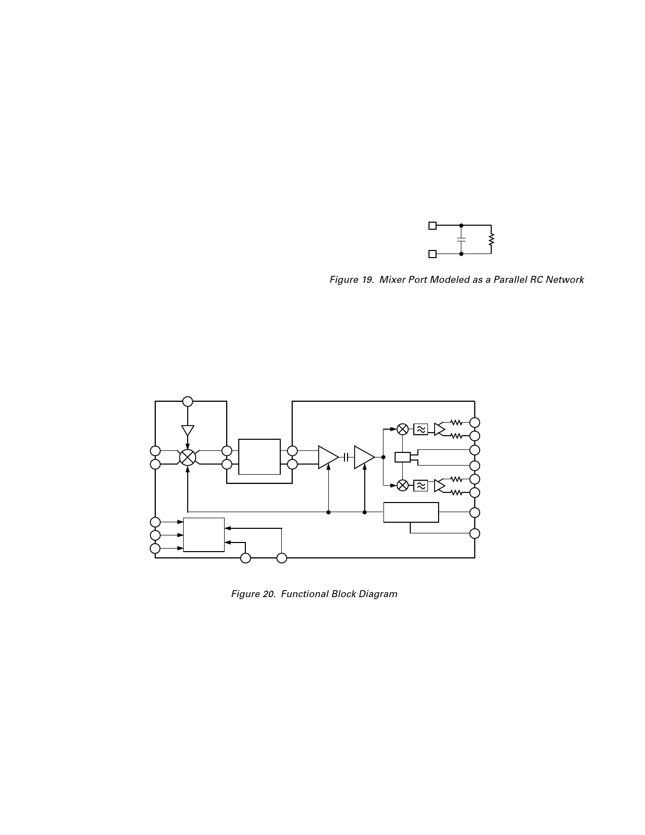
Figure 20 shows the main sections of the AD6459. It consists of
a variable-gain UHF mixer and a linear two-stage IF strip,
which together provide a calibrated voltage-controlled gain range
of more than 76 dB, followed by dual quadrature demodulators.
These are driven by inphase and quadrature clocks that are
generated by a Phase-Locked Loop (PLL), which is locked to a
corrected external reference. A CMOS-compatible power-down
interface completes the AD6459.
Mixer
The UHF mixer is an improved Gilbert-cell design and can
operate from low frequencies (it is internally dc-coupled) up to
an RF input of 500 MHz. The dynamic range at the input of the
mixer is determined, at the upper end, by the maximum input
signal level of ± 90 mV (–11 dBm in 50 Ω between RFHI and
RFLO) up to which the mixer remains essentially linear, and at
the lower end, by the noise level. It is customary to define the
linearity of a mixer in terms of its 1 dB gain-compression point
and third-order intercept, which for the AD6459 are –11 dBm
and 0 dBm, respectively, in a 50 Ω system.
The mixer’s RF input port is differential; that is, pin RFLO is
functionally identical to RFHI, and these nodes are internally
biased. The RF port can be modeled as a parallel RC circuit as
shown in Figure 19.
RFHI
RFLO
CSH
RSH
Figure 19. Mixer Port Modeled as a Parallel RC Network
The local oscillator (LO) input is internally biased at VP–0.8 V
and must be ac coupled. The LO interface includes a preampli-
fier that minimizes the drive requirements, thus simplifying the
oscillator design and reducing LO leakage from the RF port.
The LO requires a single-sided drive of ± 50 mV, or –16 dBm
in a 50 Ω system. For operation above 300 MHz, noise figure
can be improved by increasing the LO level.
RFHI 6
RFLO 5
VPS1 20
VPS2 18
PRUP 3
LOIP
4
MXOP
9
10
MXOM
LC
BANDPASS
FILTER
IFIP
11
+
12
–
IFIM
BIAS
CIRCUIT
AGC VOLTAGE
AD6459
2
COM1
7
COM2
0°
PLL
50°
GAIN TO
COMPENSATION
4.7kΩ
17 IRXP
16 IRXN
4.7kΩ
1 FREF
19 FLTR
4.7kΩ
15 QRXP
14 QRXN
4.7kΩ
13 GAIN
8 GREF
Figure 20. Functional Block Diagram
–8–
REV. 0
Share Link: 