AD6432 Ver la hoja de datos (PDF) - Analog Devices
Número de pieza
componentes Descripción
Fabricante
AD6432 Datasheet PDF : 20 Pages
| |||
AD6432
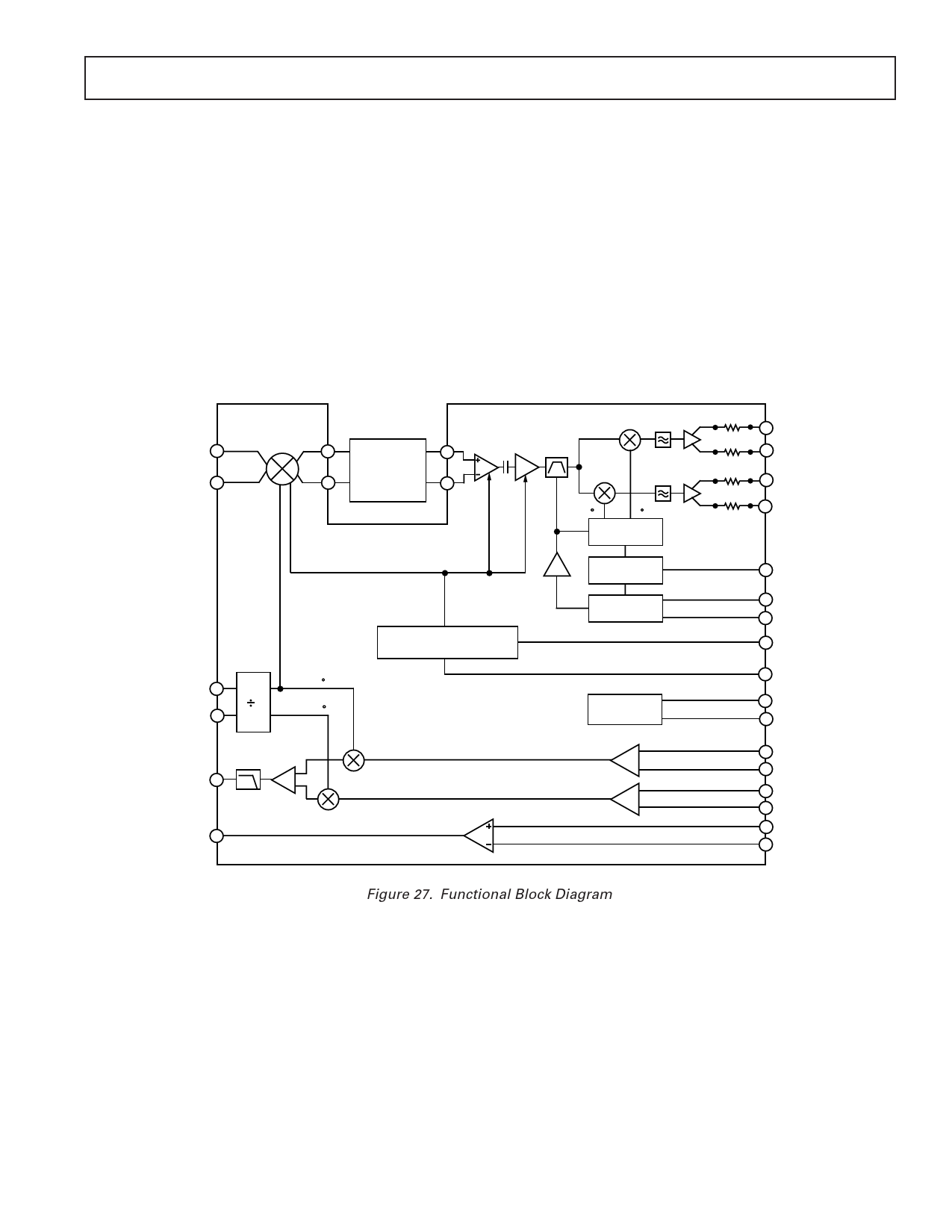
PRODUCT OVERVIEW
The AD6432 provides most of the active circuitry required to
realize a complete low power, single-conversion superhetero-
dyne time division transceiver, or the latter part of a double-
conversion transceiver, at input receive frequencies up to
350 MHz with an IF from 10 MHz to 50 MHz and transmit
frequencies up to 300 MHz. The internal I/Q demodulators,
with their associated phase-locked loop and the internal I/Q
modulator, support a wide variety of modulation modes, includ-
ing n-PSK, n-QAM, and GMSK. A single positive supply volt-
age of 3 V is required (2.7 V minimum, 3.6 V maximum) at a
typical supply current of 13 mA at midgain in receive mode and
13 mA in transmit mode. In the following discussion, VPOS will
be used to denote the power supply voltage, which will be as-
sumed to be 3 V.
Figure 27 shows the main sections of the AD6432. In the re-
ceive path, it consists of a variable-gain UHF mixer and linear
two-stage IF strip, both of which together provide a calibrated
voltage-controlled gain range of more than 80 dB, followed by a
tunable IF bandpass filter and dual quadrature demodulators.
These are driven by inphase and quadrature clocks generated
by a Phase-Locked Loop (PLL) locked to a corrected external
reference. In the transmit path it consists of a quadrature modu-
lator followed by a low-pass filter. The quadrature modulator is
driven by quadrature frequencies that are generated internally
by dividing the external local oscillator frequency by two. A
CMOS-compatible power-down interface completes the AD6432.
RFHI 10
RFLO 9
MXOP
13
14
MXOM
LC
BANDPASS
FILTER
IFIP
16
17
IFIM
0
LOHI 6
2
90
LOLO 5
MODO 2
PCAO 35
GAIN TEMP. COMPENSATION
AD6432
3MHz
90
0
QUADRATURE
VCO
DIVIDE BY
1 OR 2
PHASE
DETECTOR
RX, TX
BIAS
4.7kΩ
4.7kΩ
4.7kΩ
4.7kΩ
25 IRXN
26 IRXP
23 QRXN
24 QRXP
31 IFS0
33 FREF
29 FLTR
20 GAIN
21 GREF
19 RXPU
39 TXPU
42 ITXN
43 ITXP
40 QTXN
41 QTXP
38 PCAP
37 PCAM
Figure 27. Functional Block Diagram
REV. 0
–11–
Share Link: 