RF2418PCBA Ver la hoja de datos (PDF) - RF Micro Devices
Número de pieza
componentes Descripción
Fabricante
RF2418PCBA Datasheet PDF : 10 Pages
| |||
RF2418
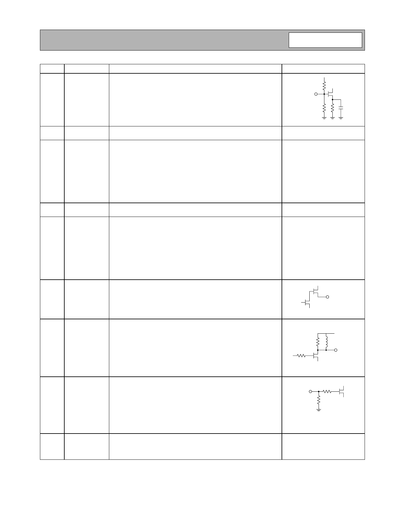
Pin Function Description
Interface Schematic
1
LNA IN A series 10nH matching inductor is necessary to achieve specified gain
and noise figure at 900MHz. This pin is NOT internally DC-blocked. An
external blocking capacitor must be provided if the pin is connected to a
device with DC present. A DC path to ground (i.e. an inductor or resis-
tor to ground) is, however, acceptable at this pin. If a blocking capacitor
is required, a value of 22pF is recommended.
LNA IN
2
GND
Ground connection. Keep traces physically short and connect immedi-
ately to ground plane for best performance.
3
VDD1
Supply Voltage for the LNA only. A 22pF external bypass capacitor is
required and an additional 0.01μF is required if no other low frequency
bypass capacitors are near by. The trace length between the pin and
the bypass capacitors should be minimized. The ground side of the
bypass capacitors should connect immediately to ground plane.
For large input signals, VDD1 may be disconnected, resulting in the
LNA’s gain changing from +11dB to -26dB and current drain decreas-
ing by 4mA. If the LNA is never required for use, then this pin can be
left unconnected or grounded, and Pin 11 is used as the first input.
4
VDD2
Power supply for the IF buffer amplifier. If the high impedance mixer
output is being used, then this pin is not connected.
5
IF BYP
If this pin is connected to ground, an internal 10pF capacitor is con-
nected in parallel with the mixer output. This capacitor functions as an
LO trap, which reduces the amount of LO to IF bleed-through and pre-
vents high LO voltages at the mixer output from degrading the mixer’s
dynamic range. At higher IF frequencies, this capacitance, along with
parasitic layout capacitance, should be parallel resonated out by the
choice of the bias inductor value at pin 7. If the internal capacitor is not
connected to ground, the buffer amplifier could become unstable. A
~10pF capacitor should be added at the output to maintain the buffer’s
stability, but the gain will not be significantly affected.
6
IF2 OUT 50Ω buffered (open source) output port, one of two output options. Pin
7 must have a bias resistor to VDD and pin 6 must have a bias resistor
to ground (see Buffered Output Application Schematic) in order to turn
the buffer amplifier on. Current drain will increase by approximately
8mA at 5V, and by approximately 5mA at 3V. It is recommended that
these bias resistors be less than 1kΩ.
7
IF1 OUT High impedance (open drain) output port, one of two output options.
This pin must be connected to VDD through a resistor or inductor in
order to bias the mixer, even when using IF2 Output. In addition, a
0.01μF bypass capacitor is required at the other end of the bias resistor
or inductor. The ground side of the bypass capacitor should connect
immediately to ground plane. This output is intended to drive high
impedance IF filters. The recommended matching network is shunt L,
series C (see the application schematic, high impedance output). This
topology will provide matching, bias, and DC-blocking.
8
LO IN
Mixer LO input. A high-pass matching network, such as a single shunt
inductor (as shown in the application schematics), is the recommended
topology because it also rejects IF noise at the mixer input. This filtering
LO IN
is required to achieve the specified noise figures. This pin is NOT inter-
nally DC-blocked. An external blocking capacitor must be provided if
the pin is connected to a device with DC present. A DC path to ground
(i.e. an inductor or resistor to ground) is, however, acceptable at this
pin. If a blocking capacitor is required, a value of 22pF is recom-
mended.
9
RF BYP Connection for the external bypass capacitor for the mixer RF input
preamp. 1000pF is recommended. The trace length between the pin
and the capacitor should be minimized. The ground side of the bypass
capacitor should connect immediately to ground plane.
IF2 OUT
IF1 OUT
Rev A7 060203
8-23
Share Link: 