PLUTO Ver la hoja de datos (PDF) - Zarlink Semiconductor Inc
Número de pieza
componentes Descripción
Fabricante
PLUTO Datasheet PDF : 15 Pages
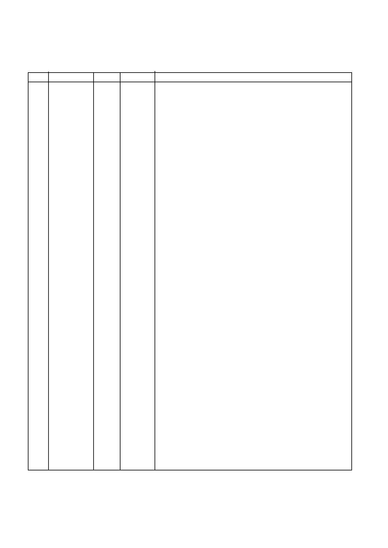
| |||
PLUTO
PIN DESCRIPTION
No
Pin Name
1
VDD
2
RSET
3
GND
4
TX_IF
5
IDLEB
6
PD TX
7
FMB
8
PD_RX
9
SLEEPB
10
RX_IF
11
TX_LOCK
12
RX_LOCK
13
TCXO/4
14
TXD<0>
15
TXD<1>
16
TXD<2>
17
TXD<3>
18
TXD<4>
19
TXD<5>
20
TXD<6>
21
TXD<7>
22
TXCLK
23
TXCLKB
24
CHIPx8
25
VDD
26
TCXO
27
GND
28
SUB
29
RESET
30
SDATA
31
SCLK
32
SLATCH
33
S<0>
34
n/c
35
RXID<0>
36
RXID<1>
37
RXID<2>
38
RXID<3>
39
S<1>
40
n/c
41
RXQD<0>
42
RXQD<1>
43
RXQD<2>
44
RXQD<3>
45
GND
46
VDD
47
RXFMSTB
48
FMCLK
49 RXQFMDATA
50 RXIFMDATA
51
ADCLK
52
ADCDATA
53
ADCENA
54
SUB
Type
Power
Input
Ground
Input
Digital
Output
Input
Output
Input
Input
Output
Output
Output
Input
Input
Input
Input
Input
Input
Input
Input
Input
Input
Input
Power
Input
Ground
Ground
Input
Input
Input
Input
Input
Output
Output
Output
Output
Input
Output
Output
Output
Output
Ground
Power
input
Input
Output
Output
Output
Output
Input
Ground
A/D
Analog
Analog
Digital
Analog
Digital
Analog
Digital
Digital
Digital
Digital
Digital
Digital
Digital
Digital
Digital
Digital
Digital
Digital
Digital
Digital
Analog
Digital
Digital
Digital
Digital
Digital
Digital
Digital
Digital
Digital
Digital
Digital
Digital
Digital
Digital
Digital
Digital
Digital
Digital
Digital
Digital
Digital
Description
Power Supply
Bias current setting resistor - 40kΩ to ground
Ground
TX VCO output
Idle mode control signal - active low - pulled low if left unconnected
TX synthesiser charge pump output
FM mode control signal - active low - pulled low if left unconnected
RX synthesiser charge pump output
Sleep mode control signal - active low - pulled low if left unconnected
RX VCO output
TX synthesiser lock detect open drain output - pulled high by ext. resistor
RX synthesiser lock detect open drain output - pulled high by ext. resistor
TCXO divided by 4 output
Transmit data bit 0 (lsb)
Transmit data bit 1
Transmit data bit 2
Transmit data bit 3
Transmit data bit 4
Transmit data bit 5
Transmit data bit 6
Transmit data bit 7 (MSB)
Complimentary Transmit Clock (+ve)
Complementary Transmit Clock (-ve)
9.8304MHz synthesiser output
Power Supply
TCXO 19.68MHz a.c. coupled sinewave input
Ground
Substrate-Ground
Chip master reset - pulled high if not connected
Serial Interface Data Input
Serial Interface Clock Input
Serial Interfce Latch Input
Aux ADC mux channel select LSB
I-Channel RX CDMA output LSB - low when inactive
I-Channel RX CDMA output bit 1 - low when inactive
I-Channel RX CDMA output bit 2 - low when inactive
I-Channel RX CDMA output bit 3 - low when inactive
Aux ADC mux channel select MSB
Q_Channel RX CDMA output LSB - low when inactive
Q_Channel RX CDMA output bit 1 - low when inactive
Q_Channel RX CDMA output bit 2 - low when inactive
Q_Channel RX CDMA output bit 3 - low when inactive
Ground
Power Supply
Receive data FM strobe - pulled low if not connected
Receive data FM clock - pulled low if not connected
Q-Channel RX FM data serial output - low when inactive
I-Channel RX FM data serial output -low when inactive
Auxiliary ADC serial data clock. Low when inactive
Auxiliary ADC serial data output. Low when inactive
Auxiliary ADC enable - pull down if not used
Substrate - Ground
2
Share Link: 