MX27L512PI-20 Ver la hoja de datos (PDF) - Macronix International
Número de pieza
componentes Descripción
Fabricante
MX27L512PI-20 Datasheet PDF : 14 Pages
| |||
FEATURES
• 64K x 8 organization
• Wide voltage range, 2.7V to 3.6V
• +12.5V programming voltage
• Fast access time: 120/150/200/250ns
• Totally static operation
• Completely TTL compatible
GENERAL DESCRIPTION
The MX27L512 is a 3V only, 512K-bit, One-Time
Programmable Read Only Memory. It is organized as
64K words by 8 bits per word, operates from a single
+3volt supply, has a static standby mode, and features
fast single address location programming. All program-
ming signals are TTL levels, requiring a single pulse. For
programming outside from the system, existing EPROM
MX27L512
512K-BIT [64K x 8] CMOS EPROM
• Operating current: 10mA@ 3.6V, 5MHz
• Standby current: 10uA
• Package type:
- 28 pin plastic DIP
- 32 pin PLCC
- 28 pin 8 x 13.4 mm TSOP(I)
programmers may be used. The MX27L512 supports
intelligent fast programming algorithm which can result
in programming time of less than fifteen seconds.
This EPROM is packaged in industry standard 28 pin
dual-in-line packages , 32 lead PLCC, and 28 lead
TSOP(I) packages.
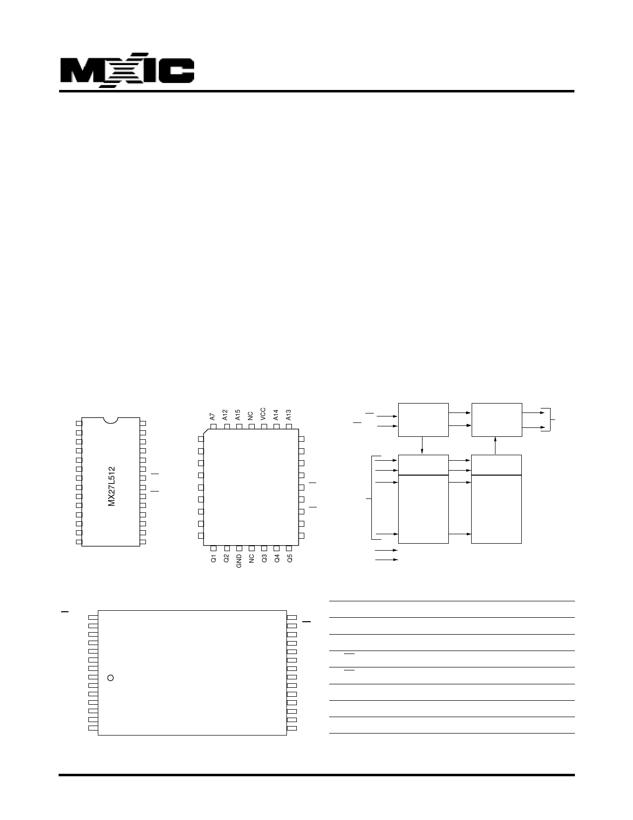
PIN CONFIGURATIONS
BLOCK DIAGRAM
PDIP
PLCC
A15 1
A12 2
A7 3
A6 4
A5 5
A4 6
A3 7
A2 8
A1 9
A0 10
Q0 11
Q1 12
Q2 13
GND 14
28 VCC
27 A14
26 A13
4
A6 5
1 32
30
29 A8
CE
OE/VPP
25 A8
A5
A9
24 A9
A4
23 A11
22 OE/VPP A3
A11
.
NC
.
21 A10
20 CE
19 Q7
18 Q6
A2 9
A1
A0
MX27L512
25 OE/VPP A0~A15
.
.
A10
ADDRESS
.
CE
INPUTS
.
17 Q5
NC
Q7
.
16 Q4
Q0 13
.
21 Q6
15 Q3
14
17
20
VCC
GND
CONTROL
LOGIC
Y-DECODER
.
.
.
.
.
X-DECODER
.
.
.
OUTPUT
BUFFERS
Y-SELECT
512K BIT
CELL
MAXTRIX
Q0~Q7
8 x 13.4mm 28TSOP(I)
OE/VPP
22
A11
23
A9
24
A8
25
A13
26
A14
27
VCC
28
A15
1
A12
2
A7
3
A6
4
A5
5
A4
6
A3
7
MX27L512
PIN DESCRIPTION
21
A10
20
CE
19
Q7
18
Q6
17
Q5
16
Q4
15
Q3
14
GND
13
Q2
12
Q1
11
Q0
10
A0
9
A1
8
A2
SYMBOL
A0~A15
Q0~Q7
CE
OE/VPP
NC
VCC
GND
PIN NAME
Address Input
Data Input/Output
Chip Enable Input
Output Enable Input/Program Supply Voltage
No Internal Connection
Power Supply Pin
Ground Pin
P/N: PM0256
1
REV. 2.6, AUG. 26, 2003
Share Link: 