MX27C1000 Ver la hoja de datos (PDF) - Macronix International
Número de pieza
componentes Descripción
Fabricante
MX27C1000 Datasheet PDF : 18 Pages
| |||
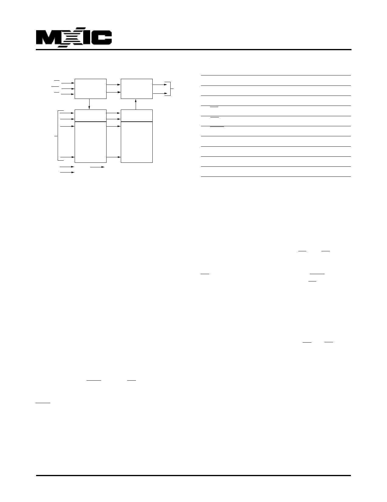
BLOCK DIAGRAM
CE
PGM
OE
CONTROL
LOGIC
OUTPUT
BUFFERS
.
.
.
A0~A16
.
ADDRESS
.
INPUTS
.
.
.
VCC
GND
Y-DECODER
.
.
.
.
.
X-DECODER
.
.
.
VPP
Y-SELECT
1M BIT
CELL
MAXTRIX
MX27C1000
Q0~Q17
PIN DESCRIPTION
SYMBOL
PIN NAME
A0~A16
Address Input
Q0~Q7
Data Input/Output
CE
Chip Enable Input
OE
Output Enable Input
PGM
Programmable Enable Input
VPP
Program Supply Voltage
NC
No Internal Connection
VCC
Power Supply Pin (+5V)
GND
Ground Pin
FUNCTIONAL DESCRIPTION
THE PROGRAMMING OF THE MX27C1000
When the MX27C1000 is delivered, or it is erased,
the chip has all 1M bits in the "ONE" or HIGH state.
"ZEROs" are loaded into the MX27C1000 through the
procedure of programming.
For programming, the data to be programmed is applied
with 8 bits in parallel to the data pins.
Vcc must be applied simultaneously or before Vpp, and
removed simultaneously or after Vpp. When
programming an MXIC EPROM, a 01.uF capacitor is
required across Vpp and ground to suppress spurious
voltage transients which may damage the device.
FAST PROGRAMMING
The device is set up in the fast programming mode when
the programming voltage VPP = 12.75V is applied, with
VCC = 6.25 V and PGM = VIL(or OE = VIH) (Algorithm
is shown in Figure 1). The programming is achieved
by applying a single TTL low level 100us pulse to the
PGM input after addresses and data line are stable. If
the data is not verified, an additional pulse is applied
for a maximum of 25 pulses. This process is repeated
while sequencing through each address of the device.
When the programming mode is completed, the data in
all address is verified at VCC = VPP = 5V ± 10%.
PROGRAM INHIBIT MODE
Programming of multiple MX27C1000s in parallel with
different data is also easily accomplished by using the
Program Inhibit Mode. Except for CE and OE, all like
inputs of the parallel MX27C1000 may be common. A
TTL low-level program pulse applied to an MX27C1000
CE input with VPP = 12.5 ± 0.5 V and PGM LOW will
program that MX27C1000. A high-level CE input inhibits
the other MX27C1000s from being programmed.
PROGRAM VERIFY MODE
Verification should be performed on the programmed bits
to determine that they were correctly programmed. The
verification should be performed with OE and CE at VIL,
PGM at VIH, and VPP at its programming voltage.
AUTO IDENTIFY MODE
The auto identify mode allows the reading out of a binary
code from an EPROM that will identify its manufacturer
and device type. This mode is intended for use by
programming equipment for the purpose of automatically
matching the device to be programmed with its
corresponding programming algorithm. This mode is
functional in the 25°C ± 5°C ambient temperature range
that is required when programming the MX27C1000.
P/N: PM0234
REV. 6.0, AUG. 26, 2003
2
Share Link: 