MX27C1000DC-45 Ver la hoja de datos (PDF) - Macronix International
Número de pieza
componentes Descripción
Fabricante
MX27C1000DC-45 Datasheet PDF : 18 Pages
| |||
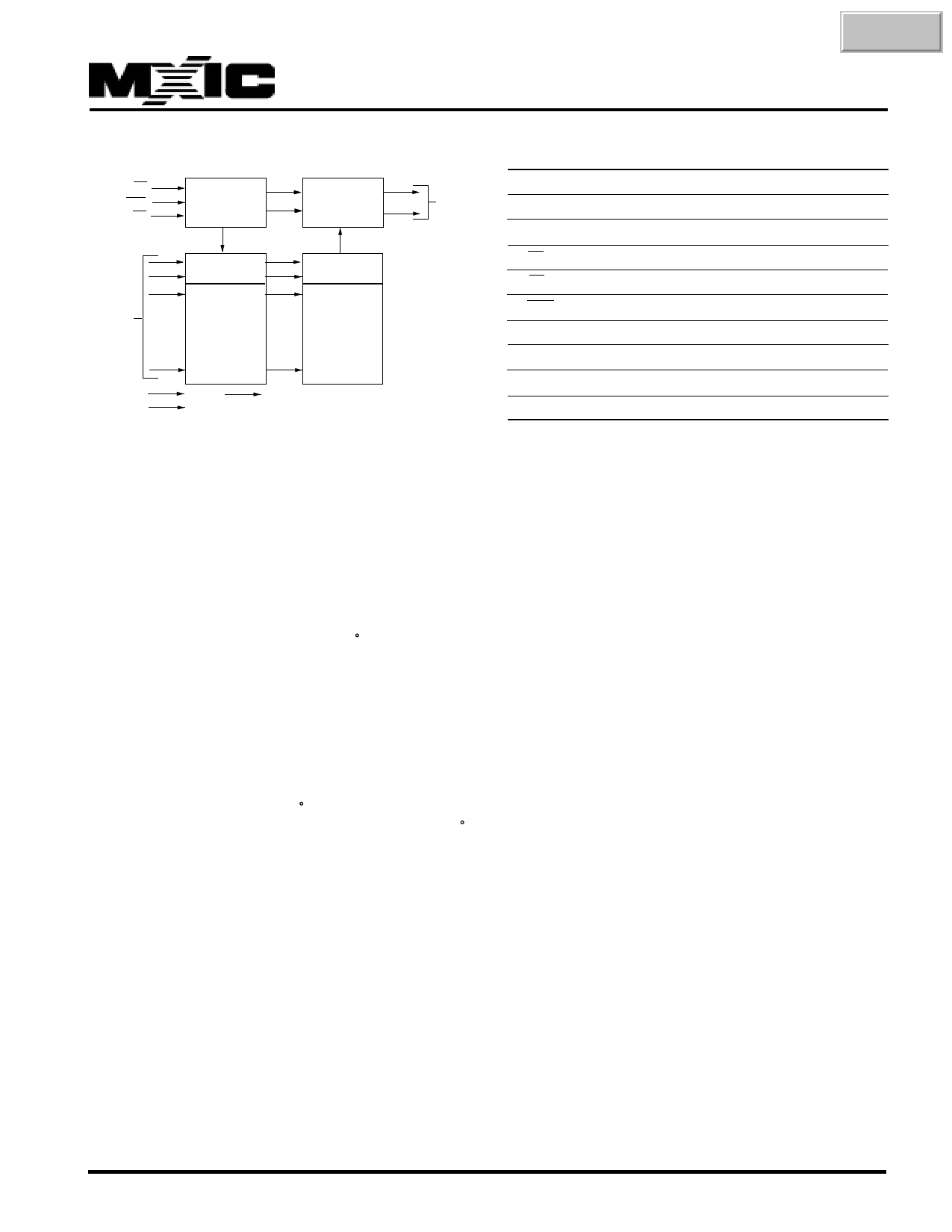
BLOCK DIAGRAM
CE
PGM
OE
CONTROL
LOGIC
OUTPUT
BUFFERS
.
.
.
A0~A16
.
ADDRESS
.
INPUTS
.
.
.
VCC
GND
Y-DECODER
.
.
.
.
.
X-DECODER
.
.
.
VPP
Y-SELECT
1M BIT
CELL
MAXTRIX
INDEX
MX27C1000/1001
Q0~Q17
PIN DESCRIPTION
SYMBOL
PIN NAME
A0~A16
Address Input
Q0~Q7
Data Input/Output
CE
Chip Enable Input
OE
Output Enable Input
PGM
Programmable Enable Input
VPP
Program Supply Voltage
NC
No Internal Connection
VCC
Power Supply Pin (+5V)
GND
Ground Pin
FUNCTIONAL DESCRIPTION
THE ERASURE OF THE MX27C1000/1001
The MX27C1000/1001 is erased by exposing the chip
to an ultraviolet light source. A dosage of 15 W seconds/
cm2 is required to completely erase a MX27C1000/1001
This dosage can be obtained by exposure to an ultraviolet
lamp - wavelength of 2537 Angstroms (A) - with intensity
of 12,000 uW/cm2 for 15 to 20 minutes. The MX27C1000/
1001 should be directly under and about one inch from
the source and all filters should be removed from the UV
light source prior to erasure.
It is important to note that the MX27C1000/1001, and
similar devices, will be cleared for all bits of their
programmed states with light sources having
wavelengths shorter than 4000 A Although erasure times
will be much longer than that with UV sources at 2537A
nevertheless the exposure to fluorescent light and
sunlight will eventually erase the MX27C1000/1001 and
exposure to them should be prevented to realize
maximum system reliability. If used in such an
environment, the package window should be covered by
an opaque label or substance.
THE PROGRAMMING OF THE MX27C1000/1001
When the MX27C1000/1001 is delivered, or it is erased,
the chip has all 1M bits in the "ONE" or HIGH state.
"ZEROs" are loaded into the MX27C1000 through the
procedure of programming.
For programming, the data to be programmed is applied
with 8 bits in parallel to the data pins.
Vcc must be applied simultaneously or before Vpp, and
removed simultaneously or after Vpp. When
programming an MXIC EPROM, a 01.uF capacitor is
required across Vpp and ground to suppress spurious
voltage transients which may damage the device.
FAST PROGRAMMING
The device is set up in the fast programming mode when
the programming voltage VPP = 12.75V is applied, with
VCC = 6.25 V and PGM = VIL(or OE = VIH) (Algorithm
is shown in Figure 1). The programming is achieved by
applying a single TTL low level 100us pulse to the PGM
input after addresses and data line are stable. If the data
is not verified, an additional pulse is applied for a
maximum of 25 pulses. This process is repeated while
sequencing through each address of the device. When
the programming mode is completed, the data in all
address is verified at VCC = VPP = 5V ± 10%.
P/N: PM0234
REV. 5.3, MAY 07, 1998
2
Share Link: 