MMJT9410 Ver la hoja de datos (PDF) - ON Semiconductor
Número de pieza
componentes Descripción
Fabricante
MMJT9410 Datasheet PDF : 5 Pages
| |||
MMJT9410
Preferred Device
Bipolar Power Transistors
NPN Silicon
Features
• Collector −Emitter Sustaining Voltage −
VCEO(sus) = 30 Vdc (Min) @ IC = 10 mAdc
• High DC Current Gain −
hFE = 85 (Min) @ IC = 0.8 Adc
= 60 (Min) @ IC = 3.0 Adc
• Low Collector −Emitter Saturation Voltage −
VCE(sat) = 0.2 Vdc (Max) @ IC = 1.2 Adc
= 0.45 Vdc (Max) @ IC = 3.0 Adc
• SOT−223 Surface Mount Packaging
• Epoxy Meets UL 94 V−0 @ 0.125 in
• ESD Ratings: Human Body Model, 3B; > 8000 V
Machine Model, C; > 400 V
• Pb−Free Package is Available
MAXIMUM RATINGS
Rating
Collector −Emitter Voltage
Collector −Base Voltage
Emitter −Base Voltage
Base Current − Continuous
Collector Current − Continuous
− Peak
Total Power Dissipation @ TC = 25°C
Derate above 25°C
Total PD @ TA = 25°C mounted on 1” sq.
(645 sq. mm) Collector pad on FR−4
bd material
Total PD @ TA = 25°C mounted on 0.012” sq.
(7.6 sq. mm) Collector pad on FR−4 bd material
Operating and Storage Junction
Temperature Range
Symbol
VCEO
VCB
VEB
IB
IC
PD
TJ, Tstg
Value
30
45
± 6.0
1.0
3.0
5.0
3.0
24
1.7
0.75
−55 to
+150
Unit
Vdc
Vdc
Vdc
Adc
Adc
W
mW/°C
W
°C
THERMAL CHARACTERISTICS
Characteristic
Symbol Max Unit
Thermal Resistance, Junction−to−Case
Thermal Resistance, Junction−to−Ambient on
1” sq. (645 sq. mm) Collector pad on FR−4 bd
material
RqJC
RqJA
42 °C/W
75 °C/W
Thermal Resistance, Junction−to−Ambient on
0.012” sq. (7.6 sq. mm) Collector pad on
FR−4 bd material
RqJA
165 °C/W
Maximum Lead Temperature for Soldering
Purposes, 1/8” from case for 5 seconds
TL
260
°C
Stresses exceeding Maximum Ratings may damage the device. Maximum
Ratings are stress ratings only. Functional operation above the Recommended
Operating Conditions is not implied. Extended exposure to stresses above the
Recommended Operating Conditions may affect device reliability.
© Semiconductor Components Industries, LLC, 2006
1
October, 2006 − Rev. 6
http://onsemi.com
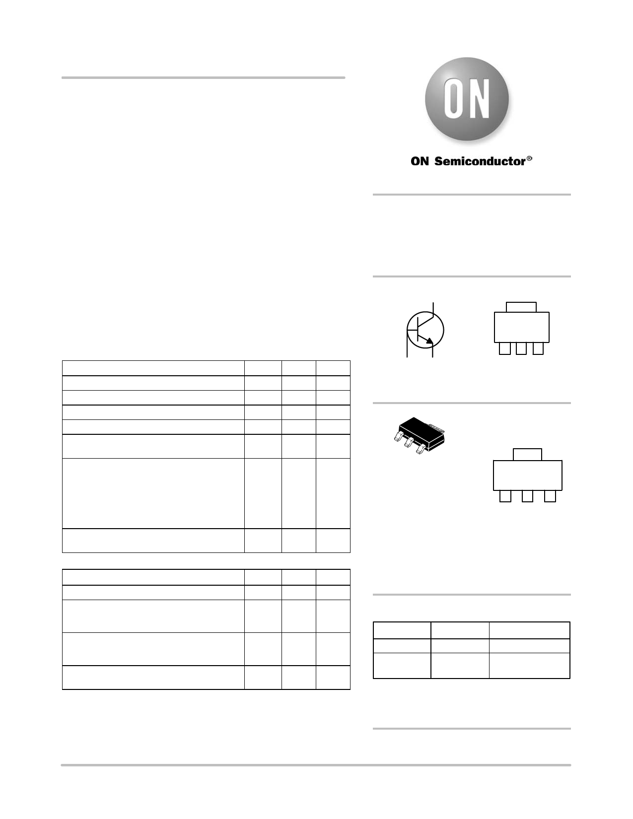
POWER BJT
IC = 3.0 AMPERES
BVCEO = 30 VOLTS
VCE(sat) = 0.2 VOLTS
C 2,4
4
C
B1 E3
Schematic
BC E
123
Top View
Pinout
MARKING
1
DIAGRAM
SOT−223 (TO−261)
CASE 318E
STYLE 1
AYW
9410 G
G
1
A = Assembly Location
Y = Year
W = Work Week
9410 = Device Code
G = Pb−Free Package
(Note: Microdot may be in either location)
ORDERING INFORMATION
Device
Package
Shipping†
MMJT9410
MMJT9410G
SOT−223
SOT−223
(Pb−Free)
1000 / Tape & Reel
1000 / Tape & Reel
†For information on tape and reel specifications,
including part orientation and tape sizes, please
refer to our Tape and Reel Packaging Specifications
Brochure, BRD8011/D.
Preferred devices are recommended choices for future use
and best overall value.
Publication Order Number:
MMJT9410/D
Share Link: 